Same-address sensors: reviewing the Qwiic Mux circuit and code
Review the pinned SparkFun Qwiic Mux design: shared power, pull-up loading, PCB routing, channel-selection behavior and practical fault recovery.
Contents
To read two I²C sensors with the same address, connect only the intended sensor's data path to the controller at each step. SparkFun's Qwiic Mux provides eight selectable branches. It neither changes the sensors' addresses nor switches their power. Selecting two same-address branches together restores the original conflict. Circuit topology, pull-ups and channel-selection software must therefore be considered together.
Imagine measuring temperature at two locations with identical sensors. An address is the identifier a controller transmits to select an I²C device. If both sensors share that identifier, it cannot distinguish them by address alone. This review follows how a switch solves that problem and which electrical and software limits remain.
Board and revision used for the review
The related assembled board is SparkFun BOB-16784, Qwiic Mux version 1.1; its manufacturer page showed in stock on 8 November 2026. For the IC, consult TI's TCA9548A product page. A bare IC needs a PCB and assembly, while a similarly named module does not establish identical connections or pull-ups.
The design source is sparkfun/Qwiic_Mux_TCA9548A at commit 9548c6af9c1a74b11904dc5b28cc3f25f7cf2ecd, dated 2 July 2020 and reviewed on 8 November 2026. Eagle, fabrication and example files were read from that revision. The README identifies version 1.1, but U2's schematic and board value is PCA9548A and its library package is named TSSOP28, although the footprint actually contains 24 pads. Before manufacturing, reconcile the actual orderable IC and its mechanical drawing; a library name does not identify an assembled part. The TCA functional reference here is TI datasheet revision H.
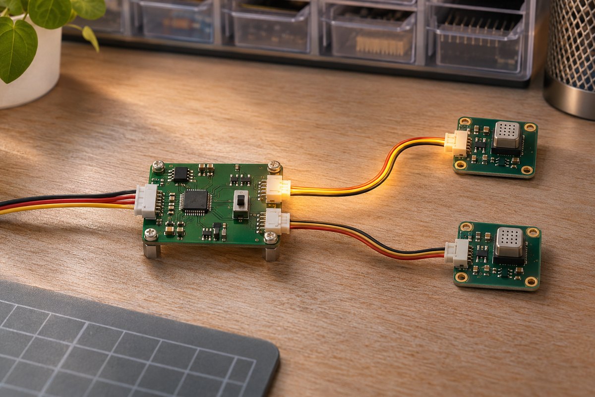
Data routing: one upstream pair and eight downstream pairs
I²C uses an SDA data line and an SCL clock line. The clock coordinates transfers of bits, the individual zero-or-one units. In this schematic, J2 and J3 both connect to MAIN_SDA and MAIN_SCL. J3 is consequently a pass-through connection to the upstream bus, rather than a ninth switched channel. U2 connects the upstream pair to separate branches: J1 is channel zero and J8 is channel one, for example.
The switch has its own address. R19, R20 and R21 are 10 kΩ pull-downs on the address inputs. Jumpers JP3, JP2 and JP1 connect A0, A1 and A2 respectively to 3.3 V. With the jumpers open, the seven-bit address is 0x70; input combinations extend through 0x77. This differs from the downstream sensor address. Changing the hub address does not separate two same-address sensors on the same connected path.
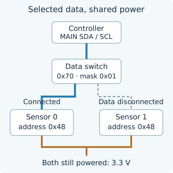
Shared power: disconnecting data does not turn a sensor off
Every connector's power pin, U2's VCC and the upper ends of the branch pull-ups share the 3.3V net. The reviewed design contains no regulator or independent branch power switch in that supply path. C1 is 0.1 µF at U2's supply; C2 through C9 are 1 µF capacitors distributed around the branch connections. A capacitor can supply part of a rapid local current change; capacitance does not establish the source's available power.
Sensor currents still add through the shared supply and connectors. Switching data does not reduce that total. Red LED D2 and its 1 kΩ resistor R24 also use this rail. The LED alone proves neither sensor communication nor adequate voltage under load. The lesson on supply branch protection helps distinguish electrical power protection from data routing.
The TCA9548A IC can support voltage translation, but this board ties its branch pull-ups and power pins to the common 3.3 V rail. It is not an assembled multi-voltage distribution system. For a different controller or sensor, reconcile line voltage, any module pull-ups and the actual input ratings. A matching connector shape is insufficient.
How the pull-ups combine
A typical I²C output drives a line low and releases it for a high level. Pull-up resistance brings the released line toward its supply. R4 and R5 provide 4.7 kΩ upstream pull-ups through JP4. Each branch has another 4.7 kΩ pair, including R6 and R7 for channel zero. Opening JP4 removes the upstream pull-up supply connections; it does not disconnect sensor power or remove every branch pull-up.
With one branch selected, and switch resistance neglected for a first approximation, two 4.7 kΩ resistors per line combine to 4700 / 2 = 2350 Ω. Selecting all eight branches with the upstream pull-up enabled gives nine parallel resistors, approximately 4700 / 9 = 522 Ω. At a low level near zero volts, approximate currents are 3.3 / 2350 ≈ 1.40 mA and 3.3 / 522 ≈ 6.32 mA. These are calculations, not board measurements. Actual switch resistance and additional sensor pull-ups modify the model. Check sinking capability against the weakest connected output's specifications.
Increasing resistance is not always better: the released line rises more slowly. Using tᵣ ≈ 0.8473 × R × C from TI's pull-up calculation guide, a hypothetical total capacitance of 100 pF gives about 398 ns with 4.7 kΩ, or 199 ns with 2.35 kΩ. Estimate or measure actual board and cable capacitance. The IC's 400 kHz clock ceiling does not guarantee satisfactory waveforms on an arbitrary cable assembly.
What the PCB arrangement tells us
The file defines an approximately 35.56 × 54.61 mm rectangular board, branch connectors along both sides and U2 near the center. It includes top and bottom copper routing and ground polygons on both layers. The upstream bus is shared between J2, J3 and U2; a cable on the pass-through port loads that bus even before a downstream channel is selected. Short PCB traces cannot compensate for arbitrarily long external cables.
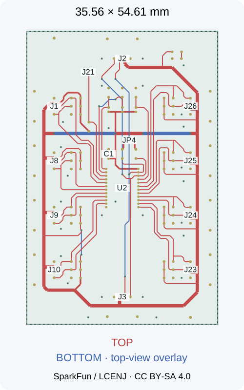
For reconstruction, inspect connector orientation, pin one, address jumpers and the pull-up jumper against the files. A CAD-derived parts list is not a confirmed purchasing BOM, particularly for U2. One proposed future layout review is to shorten C1's bypass path to U2's supply and ground pins after placement checks. The potential benefit is a smaller fast-current loop; the cost is rerouting. Placement distance alone does not prove noise or a hardware fault. Connectivity checks, DRC and voltage observations near the supply pins under load would evaluate the change.
What the example firmware actually does
Nathan Seidle's example under Firmware/Example1-BasicReadings was read at the same revision. Its header describes two accelerometers, but the current body uses one sensor object and portNumber = 4. This file does not justify a promise of two sensor outputs. Sensor-unit conversion and calibration are not functions of the mux and do not happen automatically when a channel is selected.
Mux_Control.ino contains the more consequential detail: enableMuxPort reads the existing settings and ORs in the requested channel bit. It does not clear previously enabled channels. Starting from 0x01, enabling channel one produces 0x03, connecting channels zero and one together. The main file's “this port only” comment is therefore not a guarantee provided by this helper. Multiple selection is legitimate for some applications, but same-address sensors need an explicit exclusive-selection policy.
The enable and disable helpers also ignore the return status of Wire.endTransmission() and return true after attempting the write. They detect missing data during the initial read, but a missing acknowledgement on the write can still produce a misleading success result. Input values above seven are clamped to seven; rejecting an invalid channel is clearer than silently selecting the final branch.
Proposed correction: explicit selection and observable failure
For same-address sensors, validate the channel as zero through seven, then write exactly one bit as the complete control value: 0x10 for channel four. Finish with STOP and inspect the write result. This avoids accidental accumulated selections and an extra read-modify-write operation. Its tradeoff is that it does not preserve intentionally selected additional channels.
validate channel in 0..7
mask = 1 << channel
write mask to mux address; finish with STOP
if transfer failed: report error; do not label sensor data valid
read and validate the selected sensor
optionally write 0x00 to disconnect all data channels
An address and one data byte, including acknowledgement bits, require 18 clock pulses. At 100 kHz those pulses alone occupy 180 µs. That is not the complete sensor-reading latency: start/stop timing, controller delays and clock stretching also matter. Sequentially read sensors do not provide simultaneous acquisition; retain a timestamp and validity state with each sensor's value.
If a selected branch holds SDA low, a command to deselect it may not get through the stuck bus. This design exposes !RST on J21 and pulls it toward 3.3 V with R22, 10 kΩ. Correct use provides a recovery path independent of the I²C message. Reset disconnects data channels; the faulty sensor's shared power remains present. Derive pulse timing and controller levels from the actual IC and circuit, and keep software waits bounded.
Bring-up and the limits of the conclusion
Start without branch sensors: check 3.3 V, ground and the hub address. Bring up one sensor on one branch, then add the second same-address sensor on another branch and verify exclusive selection. If a sensor remains visible unexpectedly, inspect whether it is on the upstream pass-through or whether multiple bits remain set. If added cables or modules break communication, investigate waveforms, pull-ups and supply drop rather than repeatedly scanning. The I²C troubleshooting lesson and waveform guide develop those checks.
The CAD-derived parts and connection list supports this review rather than acting as a qualified buying BOM. Hardware is released under CC BY-SA 4.0. The repository license states MIT for code while the example header includes Beerware wording; original notices are preserved in the source licence and notices file. SparkFun owns the design. The proposals are LCENJ’s editorial analysis.
Question and answer article
Ask your technical question
Questions and answers are published after moderation. Authors can see their own pending drafts.
No confirmed questions have been registered for this article yet.