TMP117 board review: why a precise sensor needs good thermal design
Review SparkFun’s TMP117 circuit and PCB: thermal isolation, supply and pull-ups, temperature conversion, a library error path and practical verification.
Contents
SparkFun’s TMP117 board converts the chip’s temperature into a digital reading. For a useful measurement, the chip must also be thermally coupled to the thing whose temperature matters. PCB slots, the power indicator, communication resistors and the way software accepts a reading all affect the result. This project illustrates why a precise sensor does not automatically make a precise thermometer.
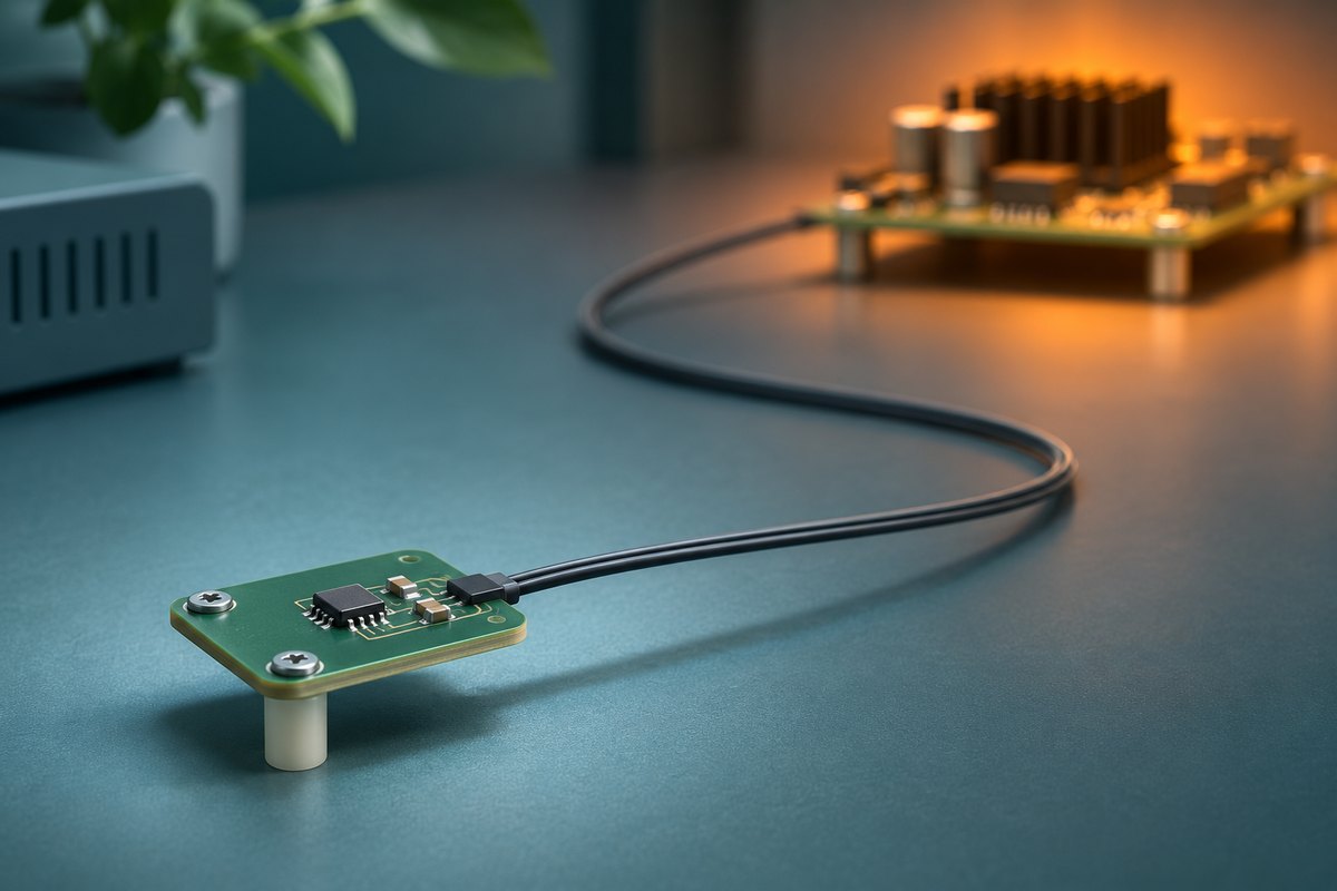
The board and package used in this review
The assembled project board is SparkFun SEN-15805. Rebuilding its PCB requires the six-pin WSON footprint used for U1; the smaller DSBGA version is not a mechanical substitute. A Qwiic cable and a host with 3.3 V logic simplify connecting this board.
This review uses the SparkFun hardware repository at commit aa763eaee71d9245e5c31daa6883f6f5c6186f16, dated November 15, 2019, with PCB marking v10. The companion library is a separate repository; its reviewed version is identified below. The work consists of design inspection and calculations, without constructing or testing a board.
First decide whose temperature you want
A digital temperature sensor reports conditions at its chip. Mounted beside a warm regulator, it can partly follow the board’s temperature rather than the surrounding air. Measuring a surface calls for thermal contact; measuring air makes unwanted heat conducted through mounting points, wires and PCB especially relevant. Choose the mounting method and location before relying on an accuracy number.
The architecture is straightforward: the host exchanges settings and readings over I2C, U1 performs the temperature conversion, and an optional alert can notify the host. There is no external analog amplifier, voltage reference or ADC in this schematic. Unlike the MCP9600 thermocouple project, this design has no remote thermocouple junction on two sensor wires: the chip itself must respond thermally to the intended environment.
Supply and the components surrounding U1
In the pinned schematic, sensor pin 5 connects to the 3.3 V net and pin 2 to ground. C1, 0.1 µF, sits across those nets. It supplies local charge during rapid current changes; it does not replace a stable power source.
J2 and J3 are Qwiic connectors and J1 is the communication header. Pins 1 through 4 are ground, 3.3 V, SDA and SCL respectively. These connections are parallel: the second connector provides neither another controller nor isolation. No regulator, logic-level translator or added protection device appears on these input paths. A 3.3 V supply and 3.3 V host logic are therefore a straightforward direct connection for this board.
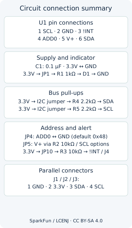
D1 is the red power indicator. R1, 1 kΩ, and the LED jumper JP1 share its branch. Assuming a 2 V LED drop gives (3.3−2)/1000=1.3 mA, drawing about 4.29 mW from the supply. This is a calculation with an assumed forward voltage, not a measured LED current. The practical lesson is that the sensor’s low current alone does not describe the complete board.
I2C resistors, address selection and the alert output
SDA is sensor pin 6 and SCL is pin 1. R4 and R5 are each 2.2 kΩ and connect to the supply through the three-pad I2C jumper. These pull-ups raise a released line; a transmitter pulls it toward ground to send a low level. Our I2C, SPI and UART comparison explains the interfaces in context.
With a line near zero volts, one pull-up carries approximately 3.3/2200=1.5 mA. Two similar boards with enabled pull-ups present 1.1 kΩ and roughly 3 mA per low line. Decide which pull-ups to retain for the entire bus; removing every pull-up does not produce a working bus either.
As an estimate, assuming 100 pF total line capacitance gives a 30–70% rise time of 0.8473RC≈186 ns in a simple RC model. Actual cable capacitance, inputs and host pull-ups change the result. Examine the waveform when diagnosing slow rising edges or an inadequate low level; reducing resistance without considering sink current is not a universal solution.
ADD0 is pin 4. JP4’s default copper bridge joins pads 2 and 3, connecting ADD0 to ground for seven-bit address 0x48. Other choices connect it to V+, SDA or SCL. Cut the default connection before selecting another: retaining ground while also bridging to SDA can ground the bus itself. With power removed, check continuity of the intended connection before changing the software address.
Pin 3 is named !INT in the schematic and ALERT in the data sheet. J4 exposes it; R3, 10 kΩ, supplies its pull-up through JP10. It can signal an alert or data readiness, but its selected role and polarity must match the register settings and host input. Basic temperature reading can instead check readiness through the register.
How the PCB limits unwanted heat
The PCB file defines a 25.4 × 25.4 mm outer boundary, with U1 at its centre, (12.7,12.7) mm. Two closed cutout paths on the Dimension layer separate its sides from the surrounding board. Thermal separation is already part of the project; adding those same slots is not a new recommendation from this review.
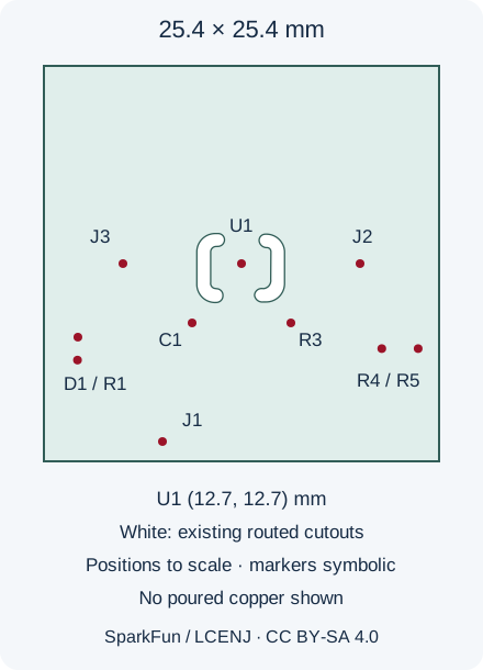
Slots restrict a solid heat-conduction path but do not eliminate thermal coupling: copper traces, board material, wires and air remain involved. C1 is below and left of the sensor, while the indicator is near the left edge. Ground polygons are defined on both copper layers; their definitions alone do not establish the final poured shape or the island’s thermal resistance.
Assembly has another important distinction. U1’s footprint contains six peripheral pads without a central paste pad. TI’s layout guidance recommends leaving the thermal pad unsoldered for high accuracy on a rigid PCB; its absence should not automatically be called a missing ground connection. During reconstruction, check pin-one orientation, all six joints and clean jumper bridges. Mechanical stress and contact with the measured object can also affect the result.
From two bytes to degrees Celsius
In SparkFun library version 1.2.5, commit c8f9b0e453ac628c013ce8af55a2501ce733cb77, dated May 25, 2023, readTempC converts the received word to a signed 16-bit integer and multiplies by 0.0078125. An invented example is 0x0C80=3200, so 3200×0.0078125=25 °C. Signed word 0xFF80 represents −128 and gives −1 °C; interpreting it as unsigned would corrupt the negative reading.
A small numerical step is not complete-system accuracy. TMP117’s ±0.1 °C specification applies from −20 to +50 °C under the manufacturer’s stated conditions; extra decimal places cannot remove mounting error or heat from nearby electronics. Our accuracy and calibration lesson develops that distinction.
What the software does, and a specific error path
The BasicReadings example starts Wire, selects a 400 kHz clock and uses begin to check both acknowledgement and device identity. The loop checks dataReady; its 500 ms delay after printing does not configure conversion time. To report matching units, read temperature once and convert that sample to Fahrenheit: this version’s readTempF calls readTempC again.
A specific problem appears in readRegister: the condition available() <= 2 enters a block containing two reads even when zero or one byte is available. The requestFrom result and the status of the register-selection transaction are not returned to the caller as communication errors. Consequently, an incomplete response can reach word construction and must not be accepted as a valid measurement. This finding comes from inspecting that function, not from disconnecting wires on a tested board.
The proposed correction separates communication success from register value. Read only after a successful transaction and exactly two received bytes, then return a success/failure status alongside the value. Mark a failed sample invalid; zero degrees is not an error code. The cost is updating callers; the benefit is preventing communication failures from entering the temperature chart. Software verification should cover zero-, one- and two-byte responses and failed register selection.
Measurable improvements and a staged first run
For low consumption or sensitivity to board heat, first examine the existing indicator. With power removed, open its LED jumper, then compare current and temperature trends before and after under the same mounting conditions. A calculated reduction in current does not prove a particular reduction in temperature error. The trade-off is losing the power indicator; the project already provides the jumper for that choice.
A second improvement is explicitly configuring conversion and averaging for the expected rate of environmental change. TI’s precision measurement application report explains how self-heating and heat exchange depend on operating conditions. In a slowly changing environment, continuous bus reads need not provide fresh information. Record sample interval, readiness and current; more averaging does not mean faster response.
Begin with power disconnected, checking jumper bridges, ground and the 3.3 V path. Connect one board, confirm its address and identity, record conversion settings and inspect several signed readings. Keep it away from hands, unintended drafts and heat sources while its trend settles. Compare against a suitable reference in the intended mounting arrangement; do not immediately turn a transient difference into a temperature-offset setting.
For no readings, start with supply, address and pull-ups. For unusual jumps, check response completeness and sample timing first. For a stable reading above a reference, investigate thermal paths, indicator and host. Offset correction is meaningful for a verified stable difference under known conditions; it cannot repair unwanted heat transfer or a broken communication path.
The hardware belongs to SparkFun; CAD notes credit Madison Chodikov and revision by Pete Lewis. This article’s circuit and placement diagrams are educational redrawings under CC BY-SA 4.0. The library’s LICENSE file states MIT while some file headers state beerware; upstream code is not redistributed here.
Question and answer article
Ask your technical question
Questions and answers are published after moderation. Authors can see their own pending drafts.
No confirmed questions have been registered for this article yet.