How a motor driver works: inside SparkFun’s hardware and firmware
Follow a two-wheel robot’s commands and motor-power paths through a SparkFun board, then examine its supply, connections, heat and firmware limits.
Contents
A motor needs both an instruction and enough electrical power to move. A control board’s signal pins carry instructions; they should not carry the motor’s operating current. A motor driver connects these two jobs: it receives a small control signal and switches the current supplied to the motor. SparkFun’s Serial Controlled Motor Driver provides a useful example of how to build that separation into a board.
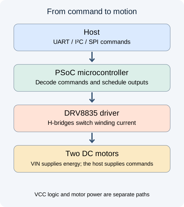
Imagine a two-wheel robot whose program asks one wheel to turn forward and the other backward. The program runs on the host—the board or computer issuing commands. This project receives those commands, interprets them in its own firmware, then uses a DRV8835 power driver to operate the motors. We will follow that path before examining power, connections, heat and software faults. A motion command does not measure wheel speed; knowing the actual speed also requires measurement feedback.
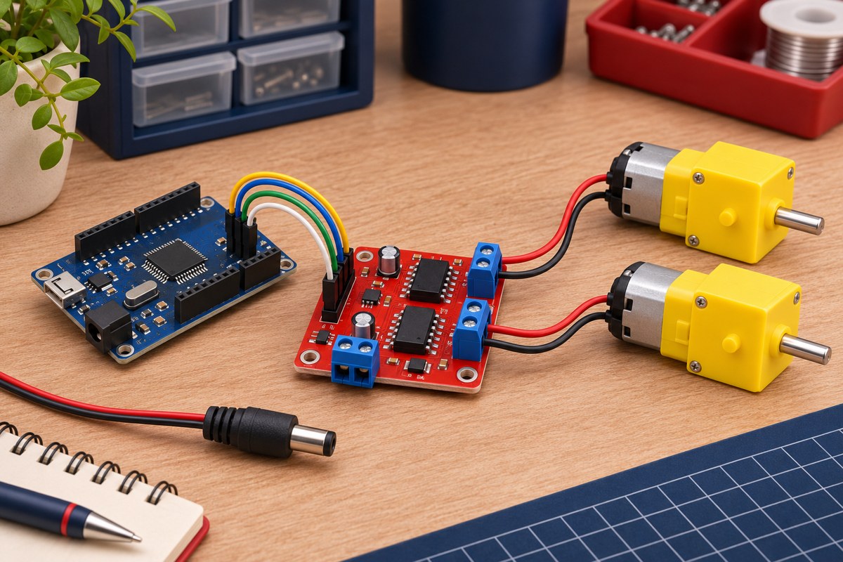
Which revision is this review about?
The design belongs to SparkFun Electronics. The schematic, PCB, SCMD document and firmware directory were read at commit 7fd71f82ea8329199dde4b64aae1c48212c2e3bd, dated 19 December 2019. That is the commit date, not this review’s date or evidence of a new release. The source’s SCMD_config.h defines firmware ID 0x7B; it does not establish what firmware is installed on a purchased board. This is a source review with independent arithmetic checks. We did not fabricate a board, compile or flash the firmware, or perform motor tests.
Three roles: deciding, interpreting and driving
Three roles make this design easier to follow. The host decides what motion is needed. The board’s PSoC microcontroller reads commands and schedules outputs; a microcontroller is a chip that runs a program, and that on-device program is firmware. The power driver switches motor current. UART, I²C and SPI are three ways of transferring data between host and board, rather than three motor-power sources.
Reversing the motor requires reversing the current through it. An H-bridge uses four electronic switches to do this. Drive strength can be varied by rapidly switching the drive on and off and changing the fraction of time it is on; this is pulse-width modulation, or PWM. Here the host sends a drive number instead of generating every pulse. Firmware stores the command in numbered locations called registers and translates it into outputs. A separate expansion I²C port and configuration-chain signals allow additional motor boards, at the cost of more startup logic and chain-dependent timing. The user and expansion ports remain separate even when both use I²C.
One input, two supply paths
Volts measure voltage difference and amperes measure current; one milliampere is one thousandth of an ampere. These units will help distinguish control-circuit consumption from motor current.
Commands alone cannot turn a motor, so the next question is where its energy comes from. The schematic—the drawing of component connections names the supply input VIN. A net is a set of electrically connected points; a repeated name identifies that connection across the drawing. In this revision VIN reaches both the motor driver’s VM pin and the regulator input. U2 is the driver’s reference label in the drawing. Capacitors C11 and C12, 0.1 µF and 10 µF, sit on this supply. A capacitor stores a small amount of charge and helps with fast changes; it does not replace a supply capable of providing motor current.
The second supply branch serves the command-processing circuitry. The SPX3819 regulator provides its supply through normally closed jumper JP5, a configurable board connection, to VCC. VCC powers the microcontroller and the driver’s logic—the circuitry that reads control inputs rather than the high-current motor output. The 1 Ω resistors R1 and R2 sit in microcontroller supply branches. They are not motor-current shunts, meaning resistors used to measure motor current, so this circuit does not establish separate current measurement for each motor.
The board is described for 3–11 V operation. The 12 V absolute limit is not a recommended operating point. A linear regulator also needs headroom above its output to regulate at 3.3 V. Near the bottom of the input range, or during a motor-starting voltage dip, do not assume VCC stays constant. For a hypothetical 11 V input and 20 mA logic-branch current, regulator dissipation is approximately (11 − 3.3) × 0.020 = 0.154 W. That current is an example assumption, not measured board consumption.
The bare SPX3819’s 500 mA headline is not the board’s permitted auxiliary output. The SCMD document gives 50 mA at the VCC output with VIN at 11 V. Nor does the regulator’s reverse-battery feature establish whole-board protection: VIN also reaches the DRV8835 directly. No series reverse-polarity diode appears in the reviewed input path.
Use the drawing to identify real connections
| Connection in this PCB | Function and qualification |
|---|---|
| J2.1 → P0.4; J2.2 → P0.5 | RX/SCL/MOSI and TX/SDA/MISO, respectively. The selected interface changes their roles. |
| J2.3; J2.4; J2.5 | Ground, SPI clock and SPI chip select. These are Eagle pad numbers, not instructions for counting pins from a photograph. |
| J4.3 → P4.0; J4.2 → P4.1 | Expansion SCL_OUT and SDA_OUT. J4.1 is ground. |
| J4.4; J4.5 | CONFIG_IN and CONFIG_OUT for chain ordering, not motor-supply wires. |
| P2.0; P2.1…P2.4 | U2 MODE, then AIN1/PH, AIN2/EN, BIN1/PH and BIN2/EN. |
| J1.1/2; J3.1/2 | Motor A’s two ends and motor B’s two ends. Connect a winding between its paired outputs; the second end is not necessarily ground. |
Having separated command and motor-power paths, check the command voltage too. “3.3 V logic” describes the supply level used by those signal circuits; it does not authorize connecting any 5 V signal directly. Use a compatible 3.3 V host interface or a level translator suitable for the chosen bus. Changing the supply through JP5 is a hardware modification that must follow the schematic to avoid tying two supply outputs together. Every component in the path matters, not only the motor driver’s voltage limit.
For UART, host TX goes to board RX, host RX to board TX, and the interfaces need a shared ground reference. This is TTL UART, not RS-232 voltage signalling. For I²C, consider the pull-ups: R7/R8 are selected to VCC through JP6; R4/R5 and JP7 serve the expansion side. Count pull-ups already present on the host and other boards before adding more. Parallel resistors reduce effective resistance and increase low-state sink current.
What the PCB shows about current and heat
The labels in the table help match the drawing to the physical board. J labels identify connectors and P labels identify chip pins; the goal is to verify each pin’s function and voltage, not to memorize names. A PCB is a printed circuit board: it holds the parts and uses copper paths to implement their connections.
The source outline is approximately 20.32 × 38.10 mm. U2 sits near the motor connectors, with four separate copper polygons carrying its outputs toward them. Those nets have no ordinary wire elements; their polygon routing must not be mistaken for missing routing. C11 is located near U2. The exposed U2 pad belongs to GND, and the file contains 44 vias on that net across the board. A via count alone establishes neither thermal resistance nor current capacity.
On a narrow screen, scroll the board view horizontally to inspect its details.
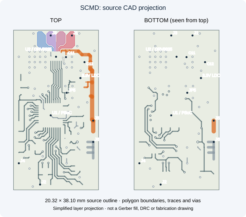
In a redesign, keep the input-capacitor, power-bridge and return-current loop short and examine motor current separately from the signal reference. Connectors, wires and copper all contribute voltage drop and heat. The small WSON package depends on its underside thermal connection; a top-side photograph cannot verify that solder joint. More copper or revised thermal-via placement is a proposal to evaluate against assembly rules, manufacturing cost and measured temperature. It should not be justified by falsely claiming that the existing board has no ground or vias.
Why 1.2 A does not mean cool operation in every enclosure
SparkFun describes 1.2 A continuous and 1.5 A peak per channel. A motor can demand much more current while starting or stalled than while spinning unloaded. Choose using its stall-current requirement and cooling conditions. Overcurrent protection and thermal shutdown do not make continuous operation near those boundaries an acceptable operating plan.
A calculation using explicit DRV8835 datasheet revision H conditions illustrates the distinction. At VCC = VM = 3 V, 0.8 A output and 25°C junction temperature, typical combined high-side and low-side resistance is 0.370 Ω. One channel’s approximate conduction loss is 0.8² × 0.370 = 0.2368 W; two equivalent channels give about 0.474 W. This excludes switching losses and the resistance increase with temperature and does not predict board temperature. The 0.305 Ω value specified under 5 V conditions must not silently replace it.
The project actually includes thermal plots. Page 9 of the SCMD document specifies 25°C ambient and equally loaded channels and compares no heatsink, a TO-220 heatsink and forced airflow. Its horizontal axis is total current across the two channels, not current per motor. These are the project author’s published tests. A board inside your enclosure still needs its own measurements.
Firmware: from a drive number to an execution time
After current paths and heating, return to the command: what number does firmware send, and when is it applied? In the source, 0x marks hexadecimal number notation; it is not a voltage or a physical unit.
Registers 0x20 and 0x21 hold the two motor commands. Startup assigns neutral 0x80, or 128. The UART drive conversion uses integer steps: 128 + direction × floor(percent × 127 / 100). Thus 50% forward becomes 191 and 50% reverse becomes 65. These percentages do not measure actual RPM or torque.
The initial UPDATE_RATE is 10, and the software counter is configured for a nominal millisecond tick. However, slaveEnumeration.c also inserts an explicit 100 µs delay after sending to each expansion board. With 16 expansion boards, those pauses alone total 1.6 ms, before wire-transfer time or other work. Selecting a 1 ms rate therefore does not guarantee that every output in a full chain updates within 1 ms.
If the host stops communicating, the last command needs an explicit recovery policy. This project provides FSAFE_TIME for a communication-loss response. Its initial value is zero, and the setting’s handler stops the timer for zero; a nonzero value configures the counter and threshold. Relevant receive paths can restart the timeout. Once it expires, interrupt code can neutralize commands or restart interfaces according to behavior bits. The presence of this code does not mean an automatic safe stop is already enabled: check the actual configuration, interrupt communication during a nonzero command with a mechanically unloaded motor, and measure stopping time. Reading the code cannot guarantee a mechanical stopping time.
A specific example bug, not a verdict on the whole product
The example also shows why a program needs a defined response when no data arrive. In Software/FailSafeTest/FailSafeTest.ino, packet[packet_ptr - 1] attempts to read the last received character. If no data have arrived and packet_ptr is zero, that index falls before the array, outside its valid memory range. This finding concerns that example program; it does not establish the same path in the board’s main firmware or predict a particular device failure time.
The proposed condition checks for a nonempty packet before access. Command-length validation and bounded ready-waits remain separate requirements. The added condition has little cost; a useful memory-checking test would cover empty input, a newline alone, truncated commands and excess-length packets. We did not run that C/C++ test or compile the project in this review.
if (packet_ptr > 0 &&
    (packet[packet_ptr - 1] == '\n' ||
     packet[packet_ptr - 1] == '\r')) {
    // Parse only after validating this command's length.
}
A bring-up process with measurable outcomes
- With power disconnected, match the components, input polarity, ground and interface jumpers to the actual board files. Select a current-limited supply and compatible low-voltage motor. Keep the wheel or mechanical load free.
- Start without a motor. Measure VIN and VCC and check the host’s signal voltage against VCC. Stop communication testing if the logic supply is unsuitable.
- Read identity and firmware version, issue neutral, and check readiness and enable status with bounded waits. A successful bus write does not prove correct motor motion.
- Start one motor at low drive. Observe current, VIN/VCC sag and actual direction. Then log temperature and repeatability with both channels and the intended load. An unloaded spin is not final load validation.
- Test host disconnection, power restoration and stall behaviour with appropriate protection and limits. Electrical and mechanical stopping times differ. This board is not an independently qualified safety controller.
If starting the motor disrupts communication, inspect supply sag and return-current paths before changing software. The related motor-noise, PWM and display troubleshooting lesson helps separate a digital symptom from a supply problem. In a new design, reverse-polarity protection and an input current limiter or fuse selected for the wiring and stall current may help. Recheck their voltage drop, motor energy returning to the supply, and the supply’s ability to absorb it. A large capacitor alone is not a guaranteed cure.
Exercise: put each of two motors’ specified no-load and stall currents beside this board’s limits. Make a test table for simultaneous starting, one stalled motor and host disconnection. Success means knowing which voltage, current and temperature you will accept, rather than merely seeing rotation. The independent calculations run 210 numerical checks and do not communicate with a motor.
Sources and design rights
- Pinned SCMD document, pages 3, 8–11, 12–15 and the register descriptions. Its expansion-pin table has ambiguous entries; the connections above were taken from schematic nets.
- Pinned main.c and devRegisters, registerHandlers, customSerialInterrupts and slaveEnumeration in the same directory; FailSafeTest is in the same repository.
- Exact PSoC product; SPX3819 datasheet revision 2.0.5 and the DRV8835 datasheet linked with the calculation.
- Repository licence: hardware CC BY-SA 4.0 and code MIT; charMath carries a separate Unlicense notice. No shop photographs were republished. Adapted and original illustration and calculation-code notices.
Question and answer article
Ask your technical question
Questions and answers are published after moderation. Authors can see their own pending drafts.
No confirmed questions have been registered for this article yet.