Inside an illuminated control knob: Qwiic Twist hardware and firmware review
Follow a click through SparkFun’s open-source board: contacts and RC filtering, ATtiny84 pins, RGB control, I2C loading and two specific firmware boundaries.
Contents
How does a control knob know whether you turned it left or right? In the open-source Qwiic Twist, two mechanical contacts indicate motion, a small microcontroller counts it, and the host reads the result over I²C. The same board handles the push-button and three-colour illumination. Its useful idea is to combine human input and visual feedback behind a simple interface—provided we understand the contacts, power supply and firmware boundaries.
This review examines SparkFun Electronics’ Qwiic_Twist repository at fixed commit f9bbde3, dated 27 August 2021. The schematic, PCB and firmware of that revision were reviewed on 30 October 2026. The associated assembled product is DEV-15083.
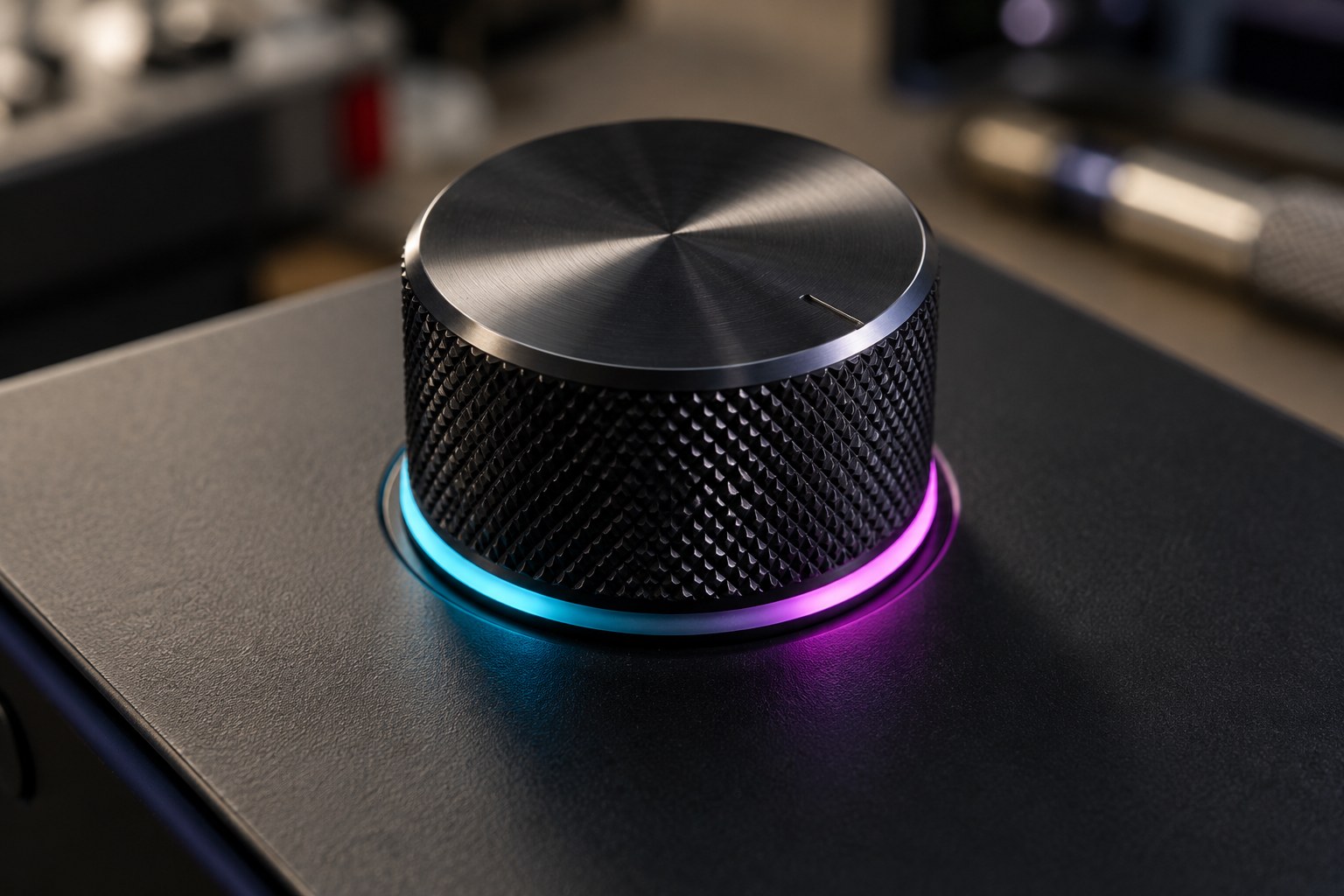
Generated educational illustration of a generic rotary control: LCENJ.
Choosing the Qwiic Twist board
This review uses the Qwiic Twist at SparkFun, DEV-15083. A bare rotary encoder is not a direct substitute: this board includes a microcontroller, firmware and an I²C interface.
The design problem: one knob, several jobs
A menu selector, brightness control or value adjustment needs rotation, a click and some feedback. Connecting everything directly to a host consumes two rotation inputs, a button input and three light outputs; the host must also follow rapid contact changes. Here U4 performs the local work and exposes values and status flags. The trade-off is an additional active component, firmware and a protocol to diagnose.
An incremental encoder counts changes; its number alone is not an absolute shaft angle. See the position-sensor and encoder introduction for references and the difference between counting and position. Likewise, keeping settings in EEPROM does not mean retaining shaft position after power loss: the running movement count is not part of the saved settings structure.
From contacts to counts: why two RC networks?
A contact is a metal connection that opens and closes as the shaft turns. The order of changes on A and B indicates direction. In the schematic, A has R4, a 10 kΩ pull-up to 3.3 V, followed by the 10 kΩ series resistor R5 and a 10 nF capacitor C3 to ground at the MCU input. B uses the equivalent R7, R9 and C1 network. The pull-up defines the open-contact state; the resistors and capacitor soften very brief transitions.
The time constant is a scale for capacitor charging speed: τ = R × C. With the contact open, charging uses both resistors: 20 kΩ × 10 nF = 200 µs. Closing the contact discharges through the series resistor: 10 kΩ × 10 nF = 100 µs. A microsecond is one millionth of a second. Calling both transitions a “100 µs filter” would therefore be inaccurate. These are ideal circuit calculations, not a guaranteed debounce time or maximum rotation speed. Actual contact bounce, input thresholds and component tolerances require measurement.
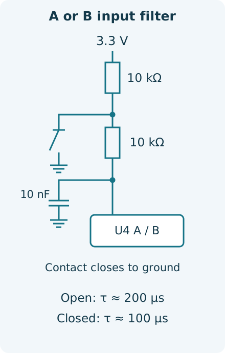
In interrupts.ino, the firmware recognises four consecutive A/B states before changing the count for a complete detent. That reduces acceptance of partial transitions; it does not prove that every bounce is rejected or every movement is counted at any speed. The push-button uses a different input: R1 pulls it down through 10 kΩ and pressing it connects it to 3.3 V. Its handler contains no explicit timed debounce interval. Button behaviour needs its own test.
Pin mapping and the host connection
Both four-pin Qwiic connectors share the bus: pin 1 is ground, 2 is 3.3 V, 3 is SDA data and 4 is SCL clock. Cable colours and board orientation are no substitute for checking pin numbers. The following physical SO14 pins of U4 come from the schematic connections; they are not the Arduino logical pin numbers used in the code.
| Function | Physical U4 pins | Circuit path |
|---|---|---|
| Supply / ground | 1 / 14 | Direct 3.3 V rail / GND |
| A / B contacts | 2 / 11 | After their RC input networks |
| SDA / SCL | 7 / 9 | Shared connector bus |
| Red / green / blue | 5 / 6 / 8 | PWM outputs and R12–R14 |
| Button / INT / address | 10 / 13 / 3 | Push-button / host notification / ADR jumper |
| Reset | 4 | R8 pull-up and programming connection |
Start with a 3.3 V logic host and common ground. The schematic contains no regulator, level translator, input fuse or TVS. The chip’s own voltage capability does not establish that the assembled board and bus are suitable for 5 V. Programming signals also share functions: BLUE connects to MISO, while the I²C lines share MOSI/SCK functions. A connected host can interfere with programming. The project instructions warn about the programmer’s default 5 V supply jumper. No programmer was connected or run during this review.
Power and RGB: appearance cannot establish current
The 3.3 V rail directly feeds U4 and the encoder LEDs’ common anode. C2 provides 0.1 µF bypassing; the 1 kΩ R3 and red D1 indicate power. With a common anode, pulling a cathode low turns its LED on. The code therefore sends 255 − brightness to PWM. PWM switches the light rapidly; its brightness number is not a calibrated current or light measurement.
The three series resistors R12, R13 and R14 are each 10 Ω in this revision. R10 is marked DNP and is not fitted. Resistance alone cannot establish actual LED current: forward voltage, MCU output voltage and duty cycle matter. The ATtiny84 datasheet specifies output-low voltage at a 5 mA load with a 3 V supply; an absolute maximum is not a design target. To assess this board, measure each colour’s current and pin voltage at fixed brightness, then all three together. The current product listing is not an independent test of this pinned PCB revision.
I²C: more than an address problem
R2 and R6 are 2.2 kΩ SDA/SCL pull-ups; three-pad jumper JP9 allows their supply connections to be cut. A pull-up raises a released line, and an output sinks current to pull it low. Approximating the low level as zero, one set draws 3.3 / 2200 = 1.5 mA. Four boards with their pull-ups enabled produce 550 Ω effective resistance and approximately 6 mA. This is an arithmetic example, not approval of a four-board connection.
A resistance that is too high, however, slows the rising edge. NXP gives tr ≈ 0.8473 × Rp × Cb. With an assumed total bus capacitance of 100 pF and 2.2 kΩ, the rise time is about 186 ns. At an assumed 200 pF it becomes 373 ns, exceeding Fast-mode’s 300 ns limit. Actual bus capacitance was not measured. Beginning at 100 kHz with short cables and a controlled pull-up population, then measuring edges and low levels, is a sensible verification path. Lower speed does not cure every bus fault.
The default firmware address is 0x3F. Closing ADR forces 0x3E; a software-configurable address is also supported within the defined range. Check electrical loading as well as addresses when adding boards. INT already has a 10 kΩ pull-up with a cuttable jumper. Firmware alternates between output-low and released input to emulate open-drain signalling. Adding this existing capability is not a new improvement.
What the PCB reveals

The individual board outline is 30.48 × 25.4 mm, with two copper layers. Four STAND-OFF library elements define mechanical mounting locations; an empty plain/hole list does not establish that mounting holes are absent. Production instructions request a 14-board panel, 1.6 mm thickness and 1 oz copper. Panel dimensions must not be reported as the individual board’s dimensions.
The A/B input routes stay on the top layer without vias. Keeping the contact-and-capacitor loop short can help clean transitions, but that benefit needs waveform verification. Bus and supply routes run between the connectors; some traces are 0.1524 mm wide. Ground has two polygons and twelve vias. Drawing a polygon is not proof of completed ground connectivity after manufacture or immunity to noise. Before reproducing the board, run pours and DRC in CAD, and inspect LED return currents, the C2 ground connection and encoder-pin clearance.
Mechanical knob loads should be carried by the assembly and enclosure rather than the Qwiic cable. Check encoder orientation, the RGB common pin, D1 polarity and SO14 orientation before soldering. Noticeable heating calls for current and short-circuit checks; route artwork cannot establish operating temperature or load capacity.
How firmware changes the hardware experience
The source register map contains ID 0x5C at offset 0, status at 1, signed 16-bit count at 5–6, count difference at 7–8 and colour brightness at 13–15. These are register offsets, not physical pins. The firmware version in this source structure is 1.2. Reading the count reports positive and negative movement; host logic must handle 16-bit wrap for long operation. Separate reads should not be assumed to form an atomic snapshot of every value.
By default, rotation notification occurs 250 ms after the last movement. For a menu indicator that follows a turning knob, polling the count is different from only waiting for this notification. Clearing status flags participates in releasing INT. The main loop uses Idle sleep rather than complete shutdown, retaining timing needed for elapsed-time tracking. Final power accounting must include LEDs, pull-ups and the host.
Settings persist in EEPROM, and the code writes changed values rather than writing on every loop iteration. Continually changing colours from the host can nevertheless accumulate saves. The datasheet specifies 100,000 EEPROM write/erase cycles. Restarting, retaining colour settings and retaining a movement count are separate tests. Pin the Core and PinChangeInterrupt dependency versions before reproducing the firmware build.
Two specific changes worth testing
Rotation boundary: in interrupts.ino / updateEncoder, the clockwise branch resets counts greater than or equal to rotationLimit to zero. The anticlockwise branch instead assigns rotationLimit itself after the count becomes negative. For a limit of 24, tracing the source gives 23 → CW → 0, but 0 → CCW → 24. This asymmetry is visible in the pinned code; it is not a measured board counting fault. If the intended contract is 0…23, use limit−1 in the second branch and restrict parameters to the valid signed-count range. The cost is changed boundary behaviour relative to the old firmware. Test both directions, limits zero, one and 24, and a round trip across zero.
Register-read boundary: receiveEvent assigns the first byte to registerNumber without validating its range. Data writes check the structure size, but requestEvent uses registerPointer + registerNumber and sizeof(memoryMap) − registerNumber without checking the offset. An offset beyond the structure creates a pointer outside the allowed registers. Validate before reading and define a bounded response for invalid offsets; a guard only in the write path is insufficient. Error behaviour must remain compatible with the host. Test the first and last valid byte and several invalid offsets. No data disclosure or device failure was observed or claimed here.
Bringing it up and checking the result
With power disconnected, check ground, supply and connector orientation. Using a suitable current-limited 3.3 V supply, record current with RGB off, then enable each colour separately and observe current and rail voltage. Identify the address and read ID 0x5C before interpreting counts. For communication failure, check power, wiring, ADR and pull-ups first; changing the position formula cannot repair a missing connection.
Next compare ten slow detents in one direction and ten back with the received count. Increase speed in steps. If counts disappear, inspect A/B at the U4 inputs and interrupt sequencing. Test the button separately through repeated presses and releases, and measure actual INT timing. Record colour, power-cycle and rotation-boundary tests separately. Agreement in one short run does not guarantee operation at every speed or noise level.
This architecture is understandable for a menu control. Precise motor-axis feedback needs the missing absolute reference and possible contact errors considered from the start. For learning the manufacturing workflow, the schematic, PCB and manufacturing-files guide separates circuit intent, board layout and fabrication outputs.
Sources and reuse rights
The primary project sources are the schematic, PCB and firmware at the same commit. Chip specifications use Atmel 8006K–AVR–10/10, pin and electrical sections; bus calculations use NXP UM10204 revision 7, section 7.1. The present product listing identifies the associated product; another revision’s files have not been substituted for the reviewed sources.
The repository hardware uses CC BY-SA 4.0, as do the derived diagrams. License.md identifies software as MIT; the original firmware header also contains public-domain/Beerware wording. All original notices remain in the unaltered pinned source archive. No separate photography licence was assumed, and no repository photographs were copied. Asset sources and modifications and the calculation and branch-trace receipt are downloadable.
Question and answer article
Ask your technical question
Questions and answers are published after moderation. Authors can see their own pending drafts.
No confirmed questions have been registered for this article yet.