MCP4725 project review: from a digital code to an adjustable voltage
How does SparkFun’s open-source MCP4725 board turn a number into a voltage? Follow its schematic, PCB, supply and I2C commands through output errors, an exercise and testable improvements.
Contents
To make a microcontroller produce, say, 1.65 V rather than simply switch a pin on and off, we can use a digital-to-analog converter, or DAC. SparkFun’s open-source MCP4725 board does this with one chip and a few supporting parts. Its central design lesson is that the number sent by software is only part of the result: supply voltage, output loading and communication timing also matter.
Voltage is an electrical potential difference, measured in volts. The microcontroller sends an integer through I²C, a serial interface with data and clock lines. The DAC converts that integer into a voltage. We will follow the problem of creating an adjustable voltage through the actual schematic and PCB, then discuss operation and verification. This board provides a low-power command signal; it is not a power supply for a motor or loudspeaker.
The exact board and purchasing options
This review covers SparkFun BOB-12918, design v14, using an MCP4725 in SOT-23-6. The schematic specifies MCP4725 without a complete orderable suffix. A reproduction therefore needs its purchased chip’s factory address option, package and operating grade checked against the datasheet. The newer Qwiic board and generic modules carrying the same chip name are separate designs.
On 29 October 2026, the direct SparkFun BOB-12918 page showed the original board as retired and out of stock. Microchip’s MCP4725 product page recommends MCP4726 for new designs; that is a reason to reassess component choice, not permission to substitute a part without checking circuitry and protocol. Regional option in Iran: the Aftab Rayaneh CJMCU MCP4725 listing showed special-order/preorder availability. It is not the SparkFun board, and the listing does not establish the exact chip package and factory address option needed for a complete match. Seller availability and delivered-part authenticity require separate verification.
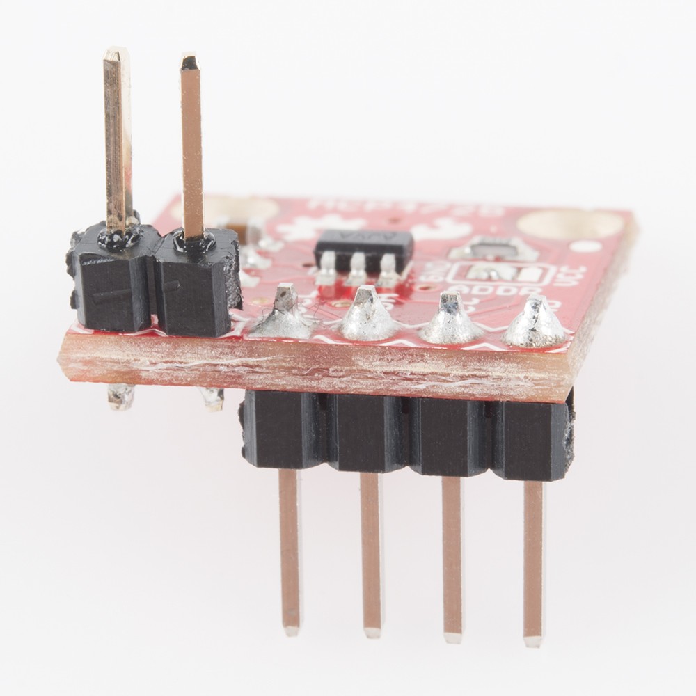
The opening photograph shows a real board with soldered headers from SparkFun’s tutorial; its physical revision was not independently established. Photo: SparkFun, Joel Bartlett’s MCP4725 hookup guide, CC BY-SA 4.0; JPEG recompressed without cropping or circuit retouching.
The reviewed revision and evidence boundary
The source is sparkfun/MCP4725_Breakout at commit 669e8aeca5987b5b91f3b7a623907a0f53e6e9fd, dated 4 February 2015, reviewed on 29 October 2026. The schematic credits Joel Bartlett and identifies revision 14. The SCH, BRD and production-panel file belong to this same revision.
This is a small hardware project. The pinned repository contains neither firmware nor a separate manufacturing BOM listing complete component ordering codes. The parts list below is reconstructed from the schematic. The exercise code is independently written by LCENJ and is not attributed to the repository.
Why this architecture solves the problem
PWM creates a pulse train with a changing fraction of on-time; obtaining a smooth voltage usually requires filtering. The MCP4725 instead holds a target code in a register, converts it with an internal resistor network and drives its output through a buffer. A buffer is an interface stage with limited load-driving capability. This allows a steady level to remain without continuous PWM generation, while leaving the usual analog accuracy limits in place.
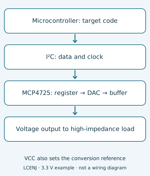
Data enters U1 through SDA and SCL, and VOUT reaches JP6. Power enters through JP5 and feeds VDD directly. The reviewed files show no regulator, independent voltage reference, or dedicated component for reverse-supply or output-overvoltage protection. Those choices help keep the board small and simple; long cables and industrial connections require protection designed for the actual environment.
Reading the schematic, pins and component list
| SOT-23-6 pin | Name | Connection in this design |
|---|---|---|
| 1 | VOUT | JP6 pin 2; analog output |
| 2 | VSS | Ground; JP6 pin 1 and JP5 pin 4 |
| 3 | VDD | VCC; JP5 pin 3 and C1 |
| 4 | SDA | JP5 pin 2 and R2 |
| 5 | SCL | JP5 pin 1 and R1 |
| 6 | A0 | SJ2 middle pad; spelled AO in the schematic symbol |
Chip pin numbers and header pin numbers are different. Establish orientation from the package’s pin-one marker and datasheet rather than mentally rotating a photograph. Also check the connector labels on the actual board: a generic module may use another pin order.
The functional parts are U1, one 0.1 µF C1 capacitor, two 4.7 kΩ resistors R1 and R2, one 10 kΩ R3 resistor, solder jumpers SJ1 and SJ2, and four-pin and two-pin headers. All three resistors and C1 use 0603 footprints. The files do not specify their tolerances, capacitor dielectric or complete ordering codes. Those details must be completed before treating this as a production BOM.
R1 and R2 pull SCL and SDA up to VCC through SJ1. Pull-ups are needed because I²C normally creates a low by pulling a line down and creates a high by releasing it. SJ1 contains default links that can be cut; pull-ups on multiple connected boards appear in parallel. Two sets of 4.7 kΩ make an effective 2.35 kΩ on each line. The disconnectable jumper is already part of the project, not an improvement invented here.
SJ2’s center pad connects to A0; one side connects to VCC and the other reaches ground through R3. The schematic note gives the default seven-bit address as 0x60 and the alternative as 0x61. Disconnect power before moving the solder selection and open the previous link according to the design. Other address bits are factory-programmed: a replacement chip’s address cannot be established from the MCP4725 family name alone.
Supply, logic levels and output loading
The chip operates from 2.7 to 5.5 V. C1 is the existing bypass capacitor between VCC and ground, providing a local path for rapid current changes. The datasheet’s typical chip supply current is 210 µA under its unloaded, code-zero condition; that is neither the whole system’s consumption nor available load current. With a 3.3 V supply, each 4.7 kΩ pull-up requires roughly another 0.7 mA while pulled low, depending on the actual low-level voltage.
Because the pull-ups connect to this board’s VCC, a 5 V supply can also make the bus 5 V. Do not connect that bus directly to a 3.3 V controller without 5 V tolerance. There is another constraint: the DAC’s minimum input-high voltage is 0.7 × VDD, or 3.5 V at a 5 V supply. Simply pulling the bus to 3.3 V therefore does not guarantee correct logic for a 5 V DAC either. Use mutually compatible supplies and thresholds, or an appropriately selected bidirectional I²C level translator.
Start by observing VOUT with a high-impedance multimeter or a suitable oscilloscope input. The main electrical table’s conditions include a 5 kΩ load and 100 pF capacitance; a 10 MΩ meter is a substantially lighter load. Short-circuit current figures and absolute maximum current ratings are not a power-delivery specification. Motors, relays, loudspeakers and difficult cable loads need an appropriate interface stage.
From a twelve-bit code to volts: resolution is not accuracy
Twelve bits provide 4,096 codes, from zero to 4,095. The datasheet’s ideal transfer is VOUT = VDD × D / 4096. At 3.3 V, the smallest ideal step, or LSB, is approximately 0.806 mV. Code 2048 gives 1.65 V, while code 4095 gives approximately 3.299194 V. The denominator is 4096, so the final code is not exactly VDD.
| Code | Output at VDD = 3.3 V | Output at VDD = 5 V |
|---|---|---|
| 0 | 0 V | 0 V |
| 1024 | 0.825 V | 1.25 V |
| 2048 | 1.65 V | 2.5 V |
| 3072 | 2.475 V | 3.75 V |
| 4095 | 3.299194 V | 4.998779 V |
These are calculations, not measurements. VDD is also the conversion reference: a hypothetical one-percent supply change shifts the ideal midscale output by 16.5 mV in the 3.3 V example, about 20.5 steps. Selecting a twelve-bit DAC or displaying three decimal places therefore does not guarantee millivolt accuracy. Offset, gain error, nonlinearity, temperature and loading must also be considered. Near the rails, do not assume the real output follows the ideal equation exactly.
What the PCB tells us about the current paths
The BRD outline is a 15.24 × 15.24 mm square. U1 is centered at approximately (7.62, 7.62) mm, C1 at (9.525, 12.065) mm, and the address jumper lies near the bottom edge. C1’s center is approximately 4.84 mm from U1’s center; this geometric distance is not the bypass loop’s actual length. Ground polygons exist on both copper layers. The rendering below follows the stored routed wires and intentionally omits ground fills and component body outlines.
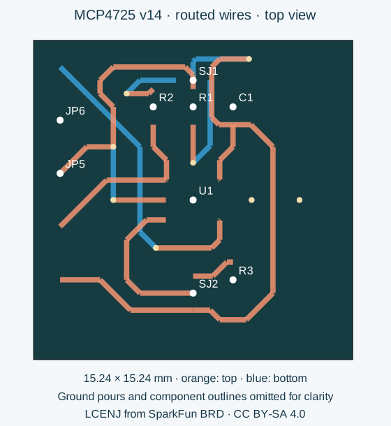
VOUT runs from U1 pin 1 to JP6 pin 2 and includes one via, an interlayer connection. SCL uses several routed segments and two vias; SDA has no vias. Via counts alone do not establish quality. A useful redesign question is whether the load’s ground reference remains short and clear of switching-current returns. A ground polygon is not a noise measurement: final assessment requires inspecting the actual pours, return paths and measured behavior.
Assembly requires checking SOT-23-6 orientation and solder bridges around the small chip, 0603 parts and jumpers. The file includes two mounting holes; metal mounting hardware must not accidentally contact copper. Under light output loading, power-stage thermal design is not the central problem, but an unsuitable load can invalidate that assumption. No PCB ampacity or connector current rating has been established by this review.
Software commands and a staged first start
The downloadable exercise targets an Arduino Uno R3 at 5 V using Arduino AVR Boards 1.8.6 and Wire. Connect 5 V to DAC VCC, common ground, A4 to SDA and A5 to SCL; connect the meter only between OUT and GND. This 5 V setup differs from the table’s 3.3 V calculation example. For another controller, review supply compatibility, pin mapping and API separately.
The datasheet’s Fast Write command takes two data bytes. In this example, the first byte’s upper four bits are zero to select the fast command and normal power mode; its lower four bits carry code bits 11–8. The second byte carries bits 7–0. Code 2048 therefore produces 0x08, 0x00. Wire takes the seven-bit address 0x60, not the shifted address 0xC0.
bool setDac(uint16_t code) {
  if (code > 4095) return false;
  Wire.beginTransmission(0x60);
  Wire.write((uint8_t)((code >> 8) & 0x0F));
  Wire.write((uint8_t)(code & 0xFF));
  return Wire.endTransmission() == 0;
}
The complete example starts the bus at 100 kHz, enables a timeout, and sends the five table codes with at least a one-second pause. Transmission errors and timeouts are reported and stop the exercise. Halting software does not necessarily set the output to zero: following an error, the actual output must be treated as unknown and a load must be brought to a safe state through an independent path. Before power-up, check VCC-to-ground shorts and jumper bridges with power disconnected. Then measure the supply without a power load and check the intermediate codes.
Fast writes do not write EEPROM. EEPROM storage uses a different command and takes typically 25 ms, up to 50 ms in the datasheet table; new write commands are ignored while it is busy. Do not write every waveform update to EEPROM. On power-up, the stored value returns, so the output is not necessarily zero before setup runs. An actuator controlled by this voltage needs an independent hardware mechanism to keep it disabled during startup.
The DAC’s typical 6 µs settling time is not the complete system’s waveform rate. Each separate transaction in this example has an address byte and two data bytes: 27 clock pulses including acknowledgements. At 100 kHz, those pulses alone take 270 µs; START/STOP timing, software and deliberate delays add more. Even ignoring that overhead, a 64-sample waveform using separate transactions is limited to approximately 58 Hz. This is a calculated ceiling, not a measured waveform frequency.
Three specific improvements, with costs and verification
1. Treat the supply reference as part of the error budget
For a stable absolute voltage, I would use a suitably low-noise supply and measure VDD at the DAC rather than assume USB provides exactly 5 V. The existing C1 stays in place. Adding bulk capacitance or a regulator requires checking that regulator’s stability and available voltage headroom, with extra cost and space. To assess the benefit, record VDD and the code-2048 output together under different host loads. Check whether output variation follows approximately half the supply variation or another error dominates. This test has not been performed here.
2. Choose bus speed from actual capacitance
For an educational assumption of 100 pF total bus capacitance, the relation tr ≈ 0.8473 × Rp × Cb in NXP’s I²C manual, pull-up selection section gives approximately 398 ns with the existing 4.7 kΩ pull-ups. That exceeds Fast-mode’s 300 ns rise-time limit, so nominal 400 kHz support does not guarantee operation with every cable and these resistors. My initial proposal is to shorten wiring and start at 100 kHz. Lower resistance may be appropriate, but low-level sink current and parallel pull-ups must be recalculated. Evaluate the result by measuring SDA/SCL rise times and acknowledgements with a low-capacitance probe; the assumed 100 pF was not measured here.
3. Design an output filter together with its load
If output steps disturb a slowly changing reference, a possible addition is a 1 kΩ series resistor followed by 100 nF to ground at the load. The simplified unloaded model has a cutoff near 1.59 kHz, but a 10 kΩ load creates a DC divider: an ideal 3.3 V input becomes 3.0 V. These values are therefore not a universal prescription. A high-impedance load or a suitable buffer can reduce that loss, at the cost of components, supply current, offset error and stability checks. Verify step response, time to the allowed error and final voltage with the real load. Neither this filter nor an added buffer exists on the original board, and neither was built for this review.
Measuring the result and locating errors
Begin with code 2048 under a light load and record both VDD and VOUT; the ideal ratio is approximately one-half. Compare codes 1024 and 3072 next. For two-point calibration, derive slope and offset from two stable intermediate measurements and validate against a third point that was not used in the fit. This can reduce linear error but does not remove nonlinearity, temperature drift or load changes. A meter with insufficient resolution cannot verify each 0.8 mV step’s accuracy.
- For missing acknowledgements, check supply and common ground, SDA/SCL, actual address and SJ1/SJ2 configuration first. Blindly changing the conversion formula will not fix the connection.
- If values track correctly but their scale is wrong, check actual VDD and whether a 3.3 V calculation is being compared with a 5 V setup.
- If connecting a load lowers VOUT, inspect load input impedance, ground drop and any series filter. The DAC is not a power source.
- If power cycling restores a different value, distinguish the volatile register from EEPROM and examine host startup timing.
- For a slow or irregular waveform, separate I²C traffic, software delays, sample count and output loading.
This project connects three concrete choices to a measurable result: where the voltage reference comes from, how the code reaches the chip and what loads the output. For the design-to-build workflow, see the schematic, PCB and manufacturing-file guide. For comparison with the opposite direction of a measurement chain, see the INA169 circuit review.
Files, references and reuse rights
The original repository archive at the reviewed commit includes the schematic and PCB with its original README and notices preserved. The README releases hardware under CC BY-SA 4.0; this article’s PCB rendering uses the same licence. Its Beerware statement about code should not be mistaken for the presence of firmware in this revision. Tutorial documentation and photographs use CC BY-SA 4.0; asset source and modification details are recorded separately.
The independent voltage-step exercise and Python calculations are by LCENJ under CC0-1.0. The Python calculations were executed. Chip specifications come from Microchip DS20002039E, February 2022, electrical tables and sections 5 and 6.
Question and answer article
Ask your technical question
Questions and answers are published after moderation. Authors can see their own pending drafts.
No confirmed questions have been registered for this article yet.