INA169 project review: from a shunt resistor to a current reading
SparkFun’s open-source INA169 board senses current through a resistor’s voltage drop. Its circuit, PCB and example code show how resistor selection, supply voltage and conversion affect the result.
Contents
A resistor opposes current flow. Measuring a circuit’s current does not always require a complicated sensor. A resistor in the power path creates a small voltage drop, from which current can be calculated. SparkFun’s open-source INA169 project turns that drop into a readable output. The central design problem is that the measuring instrument changes the circuit too: the resistor, wiring and conversion code must agree.
Current is the rate at which electric charge flows, measured in amperes; a milliampere is one thousandth of an ampere. A circuit is a set of components and connections that performs a job. A board supports those components and their copper connections. We will follow a hypothetical 10 mA load from its supply to the displayed number. A load is the device consuming power, such as a light or a small circuit. Buying hardware or running code is unnecessary to understand the example.
The reviewed board and where to buy it
This review covers SparkFun SEN-12040 and its version 1.0 design files. U1 is identified as INA169 in a five-pin SOT-23 footprint; the board file does not specify a complete orderable chip suffix. A bare chip, a generic module and this SparkFun board are different purchasing choices.
On 28 October 2026, the direct SparkFun SEN-12040 product page displayed “In stock.” For the bare device, TI’s INA169 product page identifies the device and ordering options. Regional availability in Iran: an exact matching SEN-12040 product listing and stock could not be verified in this review. A seller’s stock statement does not guarantee availability or the authenticity of a delivered item.
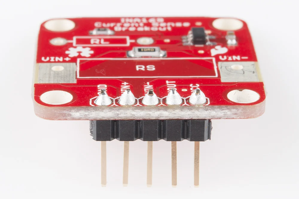
The opening photograph shows the board with soldered headers: current input and output, measurement output, supply and ground share the connector edge. Photo: SparkFun, INA169 hookup guide, CC BY-SA 4.0; converted to WebP without cropping.
Which revision and evidence are being reviewed?
The source is sparkfun/INA169_Breakout at commit 42a78dbe618fe314bf3a39a4d541c42765d4087b, dated 27 June 2025, reviewed here on 28 October 2026. The commit date does not make the circuit a new design: the schematic credits Shawn Hymel and carries a 2013 date. The schematic, PCB and Arduino example were all read from this same commit.
This is a static review of files and educational calculations. No board was built or measured, no firmware was compiled and no circuit simulation was run. Firmware is the program running on a device. A calculated result and a physical test result remain different evidence. The schematic, PCB and manufacturing-files lesson explains how the drawing relates to a board.
The solution: measure in the positive supply path
A sensing resistor, or shunt, sits between supply positive and the load’s positive input; the load’s return stays connected to supply negative. This is high-side sensing: measuring on the positive side of the supply. The shunt terminals are VIN+ and VIN−. The intended current flows from the former to the latter and creates a small voltage difference. As a starting model, voltage is the electrical push that can drive current between two points. It is measured in volts and always refers to a difference between points.
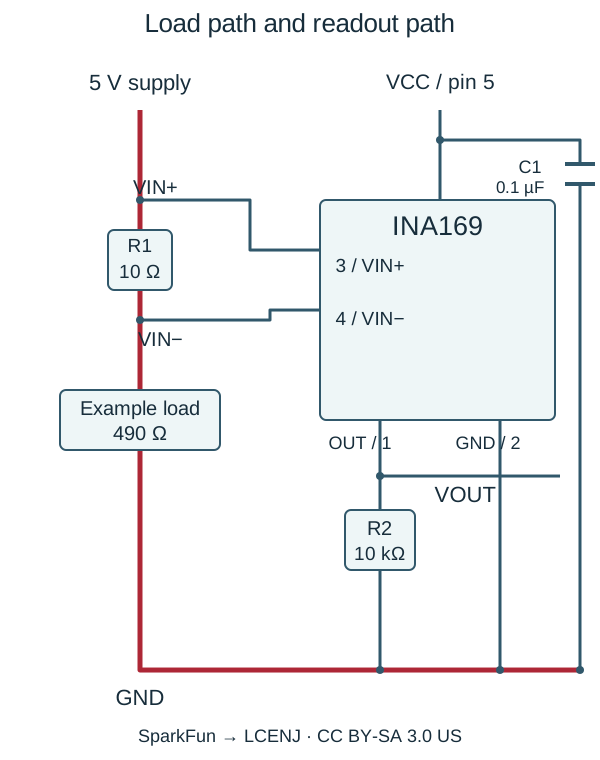
The INA169 is a chip: several electronic functions packaged in one small component. It senses the shunt voltage and produces a small current at OUT. R2 turns that current into the voltage VOUT, which a voltmeter or a computing board’s voltage input can read. The load-current path and the readout path are different: load current passes through the shunt, not through OUT.
What is actually in the schematic?
In the pinned schematic, R1 is 10 ohms and R2 is 10 kilohms. A kilohm is one thousand ohms; the ohm is the unit of resistance. R3 and R4 are alternative mounting positions, marked DNP—do not populate—in the schematic PDF. All four resistors are not intended to be fitted together.
| Actual file element | Role and assembly detail |
|---|---|
| U1 / INA169 / SOT23-5 | Pin 1 OUT, pin 2 GND, pin 3 VIN+, pin 4 VIN−, pin 5 V+. Chip pin numbers differ from the board header order. |
| R1 / 10 Ω / 1206 | Surface-mount shunt; the drawing states 1% tolerance but not a complete MPN or power rating. Package dimensions alone do not establish rated power. |
| R2 / 10 kΩ / 0603 | Converts OUT current into voltage; R4 is an optional parallel position. |
| R3 / AXIAL-0.8 | Through-hole alternative across the shunt. Include any retained resistor when calculating a changed range. |
| C1 / 0.1 µF / 0603 | Existing capacitor between VCC and GND: a small local charge reservoir for the supply, not an output-measurement filter. |
VCC powers the chip; VIN+ receives the load supply. They are not internally joined in this schematic. In a suitable low-voltage example they may be connected externally to one supply, but similar names do not establish that connection. Grounds need a common voltage-measurement reference. The measured path and reader are not electrically isolated: they share a ground reference rather than being separate electrical circuits.
Worked example: turning 10 mA into 1 V
Assume an exact 5 V supply, a 490 ohm resistive load and an exact 10 ohm R1 shunt. Treat the resistors as ideal and temperature as constant. The series path totals 500 ohms. The 1000 ohm term in the output relationship comes from the INA169 conversion scale; it is not another external resistor to fit:
I = 5 V / (490 Ω + 10 Ω) = 0.010 A = 10 mA
Vshunt = I × Rs = 0.010 A × 10 Ω = 0.100 V
Vload = 5 V - 0.100 V = 4.900 V
Vout = I × Rs × Rl / 1000 Ω
     = 0.010 A × 10 Ω × 10000 Ω / 1000 Ω = 1.000 V
Pshunt = I² × Rs = (0.010 A)² × 10 Ω = 0.001 W = 1 mW
The output voltmeter should therefore indicate about 1 V in this model; converting it back gives 10 mA. The load receives 4.9 V rather than 5 V. That 0.1 V loss explains why inserting a measuring instrument is not electrically neutral. These are predictions under the stated assumptions; resistor variation, chip error, wiring and the measuring instrument affect a real result.
Do not choose a range from one headline voltage
TI’s SBOS181F datasheet, February 2017, gives INA169 recommended supply and measured-line voltage relative to ground from 2.7 V to 60 V. The 75 V figure is an absolute stress limit; the schematic’s 75 V annotation does not authorize normal operation there. DBV denotes the five-pin SOT-23 package, and INA139 has a different voltage range. Use a current-limited low-voltage supply for this exercise.
The output cannot rise freely to any desired voltage: headroom relative to the supply and measured line limits it. The project guide suggests an approximate 3.5 to 35 mA range for 10 ohms at 5 V VCC. This is not a guarantee of identical error throughout that range, and must not be carried over unchanged to 3.3 V operation. This arrangement is unidirectional. Reverse current or AC—current that changes direction—needs more than the same board and a different software conversion.
Separate the smallest displayed change from closeness to the real current. More digits do not correct supply or resistor error. The datasheet-reading guide explains operating conditions, stress limits and typical values.
PCB layout: distinguish load paths from sense paths
INA169_Breakout.brd defines a 25.4 by 25.4 mm outline. Wide VIN+ and VIN− tracks carry load current; narrow paths toward U1 branch near the R1 pads. A pad is the copper area where a component terminal connects. This revision already separates the narrow sense routes from the broad load-current paths near R1. Higher accuracy still requires measuring the effects of pickup position, copper resistance and assembly.
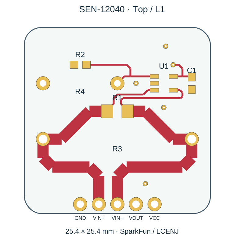
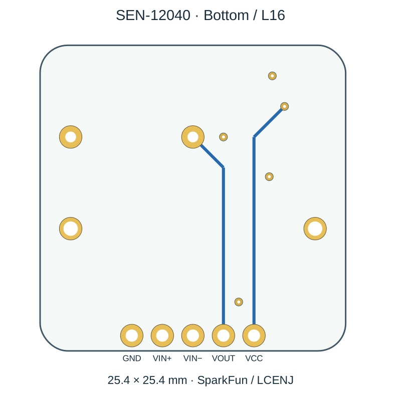
C1 already sits beside U1; their file-coordinate centres are 3.81 mm apart. Centre distance does not establish the quality of its return path. The file includes ground polygons and four ground vias—copper connections between layers. A GND label alone does not establish a noise-free reference. Part of VOUT runs on the bottom layer, connecting through R4’s plated through-hole pad. Leaving the R4 resistor unpopulated does not remove the pad’s copper connection.
A higher current range requires more than a resistor swap: dissipation, copper and lead heating, connector capability, wiring and mounting also constrain it. The full schematic contains no separate fuse, reverse-polarity protector, transient clamp or output buffer. That observation does not establish a defective board; it means these functions must not be assumed present. This exercise excludes mains and high-energy batteries.
What the example firmware assumes
The pinned Shawn Hymel example targets Arduino Uno, a board that runs a program and has voltage-measurement inputs. An ADC is the part that converts a voltage into a number. The program reads A0, assumes a 5 V reference and numbers from 0 to 1023, converts voltage to current and pauses 500 ms in each loop. It prints text over Serial, the connection used to send text to a computer, configured at 9600 baud.
In the code’s endpoint conversion model, one step is approximately 5 / 1023 = 4.89 mV. With the current gain, that represents about 48.9 microamperes per step; a microampere is one millionth of an ampere. This is step size, not guaranteed accuracy. Printing three decimal places in amperes also makes the displayed step 1 mA. A raw reading of 205 gives approximately 10.02 mA in this model and prints as 0.010 A.
The conversion hides the assumed 10 kilohm Rl in a factor of 10. Changing R2 without changing that factor gives the wrong result. VOLTAGE_REF is also declared as an integer; a fractional reference requires reviewing its type and the ADC scaling. Do not copy this conversion to an ESP32 without checking the reference, permitted input range and readout method. The 500 ms pause does not mean exactly two samples per second or reliable capture of brief peaks: reading and printing take additional time.
Three proposed improvements, with costs and checks
Change the range while considering the whole path
For a hypothetical 1 A target, a 0.1 ohm shunt instead of 10 ohms loses 0.1 V and dissipates 0.1 W. With the existing Rl, ideal output is 1 V. At 3.5 A, that resistor dissipates 1.225 W. This arithmetic is not a board or connector rating. Suitable power rating, tolerance and copper paths are required, while smaller currents produce a weaker signal. Check against a reference at several currents and inspect path temperature and voltage loss.
Resolve R1 before fitting a new resistor in R3. For example, 1 ohm in parallel with 10 ohms produces 0.909 ohms. If software assumes 1 ohm, an actual 100 mA produces an ideal reported 90.9 mA—about 9.1% low. More decimal places cannot fix that selection or assembly error.
Make the reference and conversion calibratable
Make Rs, Rl and voltage reference explicit adjustable parameters; calculate in amperes and display in milliamperes. Calibration means adjusting the relationship between a reading and a quantity using a trustworthy reference. Record several points across the range and one near zero, then repeat after warm-up. The benefit is a more traceable correction; costs include reference equipment and time. Calibration cannot recover a saturated output or repair a wrong connection.
Stabilize slow readings while accepting a slower response
For a slowly changing load, a proposed 100 nF capacitor across R2 gives an ideal 1 ms time constant and approximately 159 Hz cutoff with 10 kilohms. The time constant sets the response-time scale. Frequency means repetitions per second; the cutoff marks the roll-off in response to faster changes. This is a proposal, not an existing output component or a measured result. The capacitor attenuates fast changes too and does not by itself prevent every sampling error. Compare response time and reading spread using a known load change. A fast ADC needs its own suitable interface and settling-time design.
A proposed bring-up and troubleshooting sequence
- With power off, check the board identity, R1 and R2 values and unpopulated optional positions. Distinguish VIN+ through the shunt to VIN− from GND; do not put OUT in the load-current path.
- For this example, set a bench supply to 5 V with a 20 mA current limit and use a suitably rated 490 ohm resistive load. Supply positive goes to VIN+, then VIN− to the load, and its other terminal to supply negative. Connect VCC to 5 V and GND to the shared negative reference.
- Before attaching A0, use a voltmeter to check the shunt drop and VOUT relative to GND. The model predicts 100 mV and 1 V. If output stays near its ceiling, do not trust the linear conversion.
- For near-zero output, check power, VIN direction, load-path continuity and ground: zero output need not mean zero current. A consistent scale error suggests checking actual resistance and reference voltage. For unstable data, separate connection, supply and sampling-time checks first.
- After confirming the reader’s permitted input range, attach VOUT and compare calculation, voltmeter and current reference. These are proposed tests, not experiments performed for this article.
The optional offline Python calculation exercise checks these examples with Python 3.10 or later; it controls no device. For another sensing method, the ACS712 lesson covers zero offset and noise in a magnetic-field-based sensor. Choose according to current, acceptable voltage loss and direction requirements, rather than the number of digits alone.
Sources and licenses
- SparkFun repository at the pinned commit, with Shawn Hymel’s circuit design and version 1.0 hardware. Hardware and derivative-work license: CC BY-SA 3.0, with a US-license link in the hardware README. Adapted diagrams are LCENJ redrawings and simplifications of this revision.
- Official INA139/INA169 datasheet, SBOS181F: pins, operating limits, transfer function, output headroom and filter example. Keep INA169 claims distinct from INA139.
- SparkFun guide and photograph source, CC BY-SA 4.0. Original code retains its Shawn Hymel / SparkFun and Beerware notice. The calculation exercise here is separately written. Asset attribution details.
Question and answer article
Ask your technical question
Questions and answers are published after moderation. Authors can see their own pending drafts.
No confirmed questions have been registered for this article yet.