Inside Qwiic OpenLog: from sensor readings to reliable card files
Qwiic OpenLog records host data to a memory card. Its circuit and firmware reveal how supply dips, card stalls and incomplete error reporting affect the result, and what a more robust logger needs.
Contents
Recording a room’s temperature overnight should not require a computer to stay on. A small data logger can save readings to a memory card for later inspection. SparkFun’s Qwiic OpenLog does this over I²C, but connecting a card is only part of the design: its supply must survive writes, the host must tolerate card delays, and the software must distinguish receiving data from saving it reliably.
This review examines the SparkFun DEV-15164 board and the Qwiic_OpenLog repository at commit f3f6a3ec3f70fe4c14612b38fac360f26ee79a4c, dated May 12, 2023. The schematic, PCB and four firmware source files at that revision are the evidence. SparkFun owns the original project; the discussion below analyzes its design and proposes extensions.
Buying the board and selecting a memory card
The exact board is SparkFun Qwiic OpenLog, DEV-15164, an assembled board with an ATmega328P in a TQFP package. It is distinct from the UART OpenLog DEV-13712 and OpenLog Artemis. On October 26, 2026, SparkFun’s direct product page displayed an in-stock status. That is the seller’s observation at the check time. For readers in Iran, a verifiable direct listing and stock status for this exact board were not established; a similarly named module is not a verified substitute.
The current product page specifies 64 MB to 32 GB microSD cards formatted as FAT16 or FAT32. The pinned README makes a broader capacity claim; use the product’s documented range as the starting point. A 64 GB card in its default exFAT format is not automatically compatible because it fits the socket. A file system organizes file names and storage locations; capacity alone does not establish compatibility.
What problem does this architecture solve?
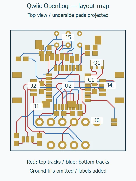
A sensor converts a physical property, such as temperature, into a readable value. A host board reads that value and decides what to record. Its microcontroller is a small chip that executes a program and communicates through electrical pins. OpenLog does not independently collect every sensor reading: the main host must send the data. Having two Qwiic sockets does not make it a controller that polls a neighboring sensor.
I²C transfers messages using two lines: SDA carries data and SCL establishes the timing. Here, the host initiates commands and OpenLog responds. OpenLog’s processor then controls the card through a different interface, SPI. This division moves file handling away from the host, but does not remove delays or errors. The I²C troubleshooting lesson explains a useful connection and response-checking sequence; its ESP32 pin numbers are not this board’s pin map.
Power: this board takes 3.3 V
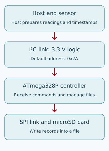
In the pinned schematic, the 3.3 V rail directly supplies U2’s VCC and AVCC, card socket J1, and Qwiic connectors J2 and J4. There is no 5 V-to-3.3 V regulator on that path. Do not connect a 5 V supply or 5 V logic directly. Use a suitable regulated supply, a common ground and a host compatible with 3.3 V signaling. Programming connector J6 shares the supply too; do not tie two supply outputs together without reviewing their behavior.
C1 is 4.7 µF and C3 is 0.1 µF across supply and ground. A capacitor stores electrical energy and can provide some local current during rapid changes. It does not replace a suitable supply or low-resistance connections. The manufacturer’s guide gives roughly 20–23 mA while writing, depending on the card. Do not treat that figure as a guaranteed peak-current limit for every card.
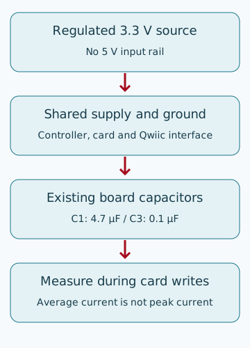
For a hypothetical example, supporting a 50 mA load for 20 ms with a 0.3 V allowable drop requires an ideal C = I × Δt / ΔV = 0.05 × 0.02 / 0.3 ≈ 0.00333 F, about 3330 µF. This is not a finished capacitor selection: equivalent series resistance, startup current, minimum card and processor voltage, power-fail detection and actual write-completion time remain to be established. The existing 4.7 µF capacitor is not a guaranteed hold-up supply for every power interruption.
Bus wiring, pull-ups and the processor clock
SDA connects to processor pin PC4 and SCL to PC5. R5 and R4 are each 2.2 kΩ, connected to 3.3 V through the I2C jumper. These pull-up resistors raise a released line. With a low voltage near zero, each draws approximately 3.3 / 2200 = 1.5 mA. Two boards each contributing 2.2 kΩ yield 1.1 kΩ in parallel and roughly twice the current. Review the combined pull-ups and each device’s ability to pull the line low; a chain of boards does not necessarily need every pull-up enabled.
The default seven-bit address is 0x2A. Closing ADR pulls PD3 low, and startI2C then forces address 0x29. This firmware also has a software address-setting path. Configure multiple units separately before placing them on the same bus, and check the interaction of config.txt and EEPROM after a restart. An address, a voltage and a physical pin number are different things.
The schematic identifies Q1 as a 16 MHz resonator; the guide’s informal crystal wording does not change that component designation. In the ATmega328/P data sheet, Speed Grades section, maximum frequency depends on supply voltage. The 16 MHz, 3.3 V point is outside the chart’s guaranteed operating region. This matters when reusing the design; it is not evidence that every board fails. A new revision could investigate a compliant lower clock, with corresponding changes to F_CPU, bootloader, UART and SPI timing, and I²C service capacity. Raising the whole board to 5 V is not a solution because the card and interfaces share that rail.
What the PCB reveals
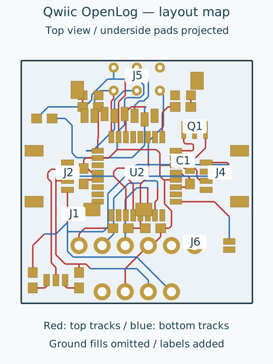
In the board file, U2 is at (12.7, 13.97) mm and Q1 at (19.05, 19.05) mm. Card socket J1 is on the underside, with J2 and J4 on opposite sides. The SPI nets connect PB3 to card DI, PB4 to DO, and PB5 to SCK. PB2 selects the card, with R3 providing a 10 kΩ pull-up. That resistor helps keep the card deselected while the pin is released; correct initialization is still necessary.
Ground polygons are defined on both copper layers, but their presence does not prove that every return path is continuous. Inspect the filled output and the actual card-current path in a PCB tool. C1 sits near the card region. In an extension, keep its power and ground connections short and avoid sharing a narrow card-current return with a sensitive sensor reference. Green LED D3 is connected to SCK through 330 Ω resistor R6. Its flashing indicates clock activity, not a valid file or durable data. Preserve the resonator’s proximity and short clock routes in a redesign.
How does this firmware actually write data?
Qwiic_OpenLog.ino reports firmware version 3.1 at the reviewed commit. Its command table maps register 0x0C to writeFile and 0x11 to syncFile. Here a register is a message code telling the board what to do with the remaining bytes. The expected Wire message buffer is 32 bytes. One byte selects the command, leaving at most 31 data bytes in a conventional message. The host library must split longer transfers appropriately.
The incomingData array allocates 257 bytes, but receiveEvent clears the array and resets its position for each message, then calls the command handler immediately. It is not a continuous 256-byte queue absorbing card stalls. File operations execute on the I²C receive-callback path. When the card stalls, the host needs compatible clock-stretching and timeout behavior. Selecting a 400 kHz bus clock does not guarantee a steady logging rate. Moving operations to a main-loop queue would also require a reviewed acknowledgement, congestion and concurrency design.
In commands.ino, writeFile obtains the length using strlen. This stops at the first zero byte: a hypothetical payload 41 00 42 has a computed length of one, not three. Plain-text logging and arbitrary binary logging are therefore different use cases. Binary support needs an explicit-length protocol and implementation review, or host-side text/encoding conversion with its additional storage overhead.
Calculate the workload before choosing a rate
Suppose each record, including its sequence number, timestamp, temperature and line ending, is exactly 24 bytes, with ten records per second. The data rate is 24 × 10 = 240 byte/s. One day produces 240 × 86400 = 20,736,000 byte, about 20.7 decimal MB, excluding file-system overhead. Count your actual formatted records rather than assuming they have this size. Each hypothetical line fits within a 31-byte payload, but command and address bytes and acknowledgement bits still consume bus time.
A second hypothetical application generating 1000 samples per second at 16 bytes per sample needs 16,000 byte/s. That approaches the product page’s roughly 20,000 byte/s claim, which is not a guarantee for every card and transaction pattern. Even a genuine 256-byte queue would cover only 256 / 16000 = 0.016 s, or 16 ms, at that rate. The current array is not such a queue. For continuous vibration or audio capture, measure the longest card stall and congestion tolerance and design around worst-case latency rather than average throughput.
Power loss: reception is not enough
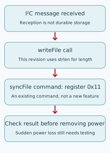
writeFile ignores workingFile.write’s result and then sets the success bit. syncFile likewise ignores the return from sync and announces success. In this revision, that bit alone therefore does not establish a complete write or successful synchronization. A specific improvement is to compare bytes written with bytes expected and report synchronization errors. The host must read and handle that status too. Blind retries can duplicate records.
MAX_IDLE_TIME_MSEC is 500, but the idle branch of loop disables peripherals and sleeps; it does not call workingFile.sync there. A variable name or an older comment is not proof that data is reliably committed every 500 ms. Explicit synchronization, an orderly shutdown and adequate power are needed. Even a successful sync is not a universal power-loss guarantee: the card controller’s behavior and possible file-system damage still require separate testing.
Concrete improvements and their costs
| Evidence and need | Proposed change and cost | How to evaluate it |
|---|---|---|
| Card and processor share 3.3 V power. | Use a supply with suitable transient capacity; consider energy storage and power-fail detection. Costs include parts, area and startup current. | Capture voltage at J1 and U2 during startup and writes. Use expendable test data and a test card for controlled power interruptions. |
| writeFile and syncFile do not inspect their results. | Report actual byte counts and errors. Update the host/logger contract together. | Inject short writes and sync failures in software tests; then assess absent and full cards on test hardware. |
| File operations run inside the receive callback. | For latency-sensitive hosts, investigate a bounded queue and main-loop processing. This consumes RAM and requires busy/congestion handling. | Measure worst-case latency and host timeouts with target cards. Sequence numbers reveal missing or duplicate records. |
| strlen truncates at the first zero byte. | Define explicit-length binary framing or store encoded/text records, with additional size and conversion costs. | Compare files against zero-containing, empty, 31-byte and multi-message inputs. |
| 16 MHz at 3.3 V requires a guaranteed-operating-region review. | Choose a compliant clock, firmware and bootloader for a new design. Lower frequency may reduce processing capacity. | Review worst-case voltage/temperature, interface timing and logging rate. One working sample does not replace data-sheet limits. |
A practical bring-up and evaluation sequence
- Identify the exact board and card format. With power disconnected, check orientation, ground and shorts. Begin without long cables or additional loads.
- Power it from a suitable 3.3 V source and measure voltage beside the card. For a 5 V host, resolve supply and signal compatibility separately; a connector fitting is not proof of compatibility.
- Check only address 0x2A, or 0x29 with ADR closed, first. Then read card-initialization and file-open status. An I²C acknowledgement establishes a responder’s presence, not a functioning storage chain.
- Write a few short numbered lines, request the existing sync operation and finish cleanly. Remove the card after safely disconnecting power and compare its line count and content on a computer.
- Increase the rate gradually, recording latency, missing records and duplicates separately. Have the host include acquisition timestamps; this design has no on-board real-time calendar clock.
- After normal operation works, assess card faults and controlled power loss using disposable data. Define acceptance first: how much loss is acceptable, and what recovery is required after power returns?
The firmware dependency notes recommend SdFat 1.1.4 or a pre-2.x release and also require SerialPort. Included HEX files do not establish that a historical binary can be reproduced with current libraries. No firmware compilation or hardware execution was performed for this review; the findings come from circuit, layout and source inspection plus arithmetic checks. For a physical build, select and record a compatible version of the separate SparkFun host library; that dependency repository is not the hardware commit.
Sources, calculation file and review limits
The worked-example calculation file performs ten arithmetic checks. It does not simulate a circuit or card. The schematic, PCB and main firmware paths were read at the named commit. No board was built or flashed; no physical measurements, noise testing or power-loss endurance testing were performed. Firmware development is optional advanced work requiring AVR programming knowledge. Understanding the design does not depend on buying hardware or running code.
The hardware belongs to SparkFun Electronics, and the firmware header credits Nathan Seidle. The repository license identifies hardware as CC BY-SA 4.0 and software as MIT; retain and review the main source header’s public-domain/Beerware wording when reusing files. The explanatory figures are redraws, not board photographs. Their license and changes are available separately. This project is useful because its files expose the complete path from a sensor reading to a file, including the gap between ordinary operation and predictable failure handling.
Question and answer article
Ask your technical question
Questions and answers are published after moderation. Authors can see their own pending drafts.
No confirmed questions have been registered for this article yet.