NE555 Monostable Timer: Pinout, Circuit and RC Timing
Learn NE555 pin functions, build a 5 V one-shot, calculate RC pulse width and check tolerance, with a real photo, schematic and component purchase links.
Contents
The NE555 creates timed pulses without software. In a monostable circuit, a short trigger makes the output active for approximately t ≈ 1.1RC. This tutorial uses the Texas Instruments NE555P at 5 V and a nominal 1.1-second example. Actual pulse width depends on the components, trigger waveform and operating conditions.
Buy the NE555P: manufacturer, distributor and Iran options
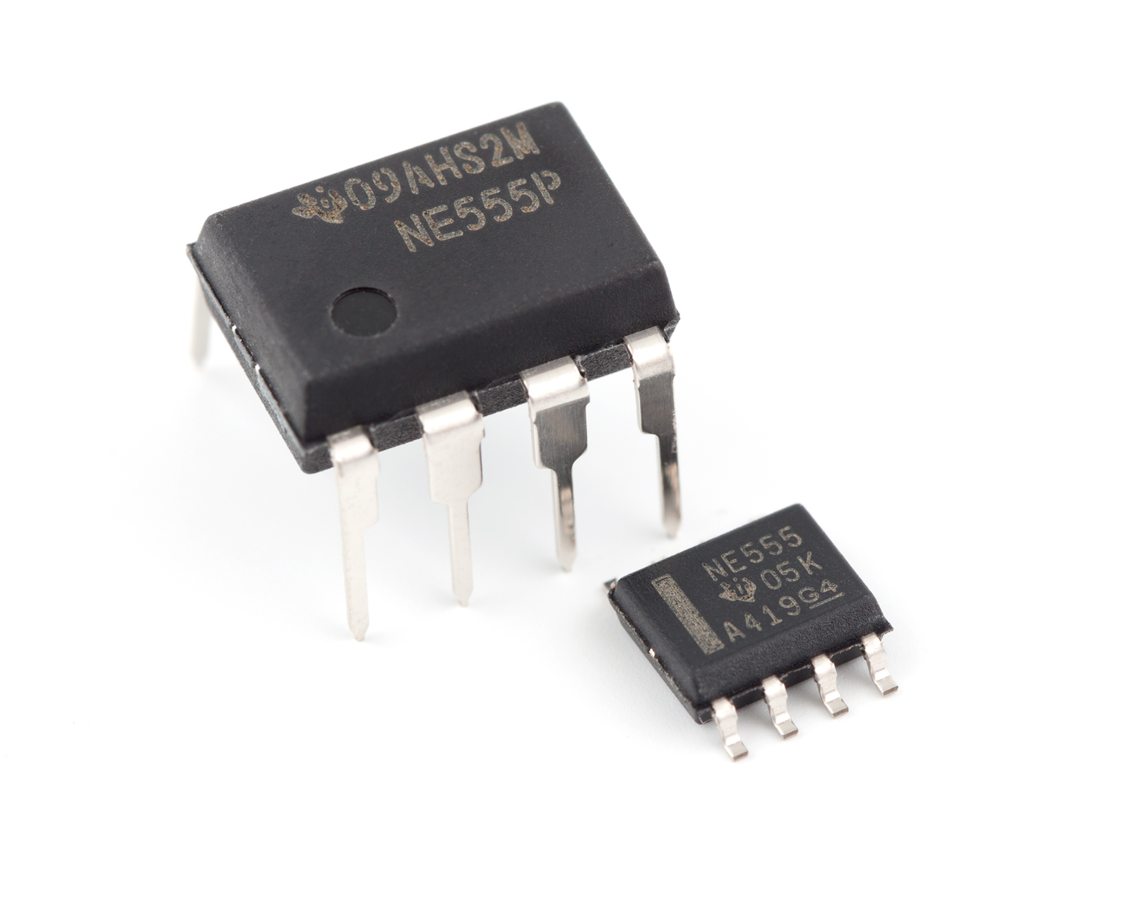
The reference part is Texas Instruments NE555P, PDIP-8. A breadboard needs the through-hole package; an SOIC device is a different physical part. The links below go directly to product pages.
| Supplier | Direct product link | Verification and availability |
|---|---|---|
| Texas Instruments | Order the exact NE555P from TI | Exact ordering code and package. Check current inventory and destination-specific shipping when ordering. |
| DigiKey | NE555P, distributor code 296-NE555P-ND | Direct page for the same MPN and PDIP-8 package. Inventory and delivery conditions can change. |
| Iran: ECA | NE555 DIP timer from an Iranian seller | The product page displays in-stock status, checked on 15 October 2026. Its title says NE555 DIP and its specifications name TI and PDIP-8; the complete NE555P ordering code on the delivered device has not been independently verified. |
Seller availability is a dated observation, not a stock, authenticity or delivery guarantee. Match the manufacturer, package and device marking before ordering. No fixed price is quoted.

What does monostable mean?
Imagine an output that normally stays off. An event turns it on for a limited interval, after which it returns to its original state. That is the one-shot, or monostable, application: it can indicate an event, stretch a short pulse or create a timing window.
An astable circuit instead produces a repeating waveform. The one-shot here needs a new trigger after the previous pulse ends. It is therefore useful to distinguish a timed event from a continuously running oscillator or a programmable PWM peripheral. For the repeating-waveform case, read PWM frequency and duty cycle.
NE555P pinout: check package orientation first
The following numbers refer to the top view of the eight-pin package. Locate the notch or pin-one mark before inserting the chip; a bottom view reverses the apparent order. A schematic symbol is a map of electrical functions, not a drawing of the physical pin positions. Compare it with the NE555 datasheet pin configuration.
| Pin | Name | Role in this example |
|---|---|---|
| 1 | GND | Common ground |
| 2 | TRIG | Short active-low trigger |
| 3 | OUT | Timed output |
| 4 | RESET | Active-low reset; tied to 5 V here |
| 5 | CONT | Threshold control; 10 nF to ground |
| 6 | THRES | Timing-capacitor voltage sensing |
| 7 | DISCH | Timing-capacitor discharge |
| 8 | VCC | 5 V supply in this example |
How a charging capacitor becomes a timed pulse
While the circuit waits, an internal discharge path holds the timing capacitor near ground. A valid trigger activates the output and opens that discharge path. The resistor then charges the capacitor. Reaching the end threshold switches the output off and discharges the capacitor again.
The nominal 555 start and end thresholds are approximately one-third and two-thirds of the supply: about 1.67 V and 3.33 V on a 5 V rail. These are nominal reference levels, not guaranteed limits for every device. The capacitor does not need to reach the full 5 V supply to finish the pulse. The official LM555 monostable explanation provides another reference for this family mechanism; the example's part-specific limits and pinout are checked against the NE555 documentation.
A 5 V one-shot with a nominal 1.1-second interval
The example needs one NE555P, a 100 kΩ timing resistor, a 10 µF timing capacitor rated for at least 10 V, a 10 kΩ pull-up resistor, a 100 nF ceramic bypass capacitor and a 10 nF control-pin capacitor. Record the timing capacitor's type and tolerance when selecting it. These values form an educational starting point, not a qualified production design.
- Connect pins 8 and 4 to 5 V, and pin 1 to common ground.
- Join pins 6 and 7 to form the timing node. Connect 100 kΩ from 5 V to this node and 10 µF from the node to ground. With a polarized electrolytic capacitor, its positive lead goes to the timing node and its negative lead goes to ground.
- Pull pin 2 up to 5 V through 10 kΩ. Use a compatible pulse source to pull this input near 0 V for about 5 ms, then release it or return it to 5 V. Connect the source ground to the circuit ground. Leave at least three seconds between triggers.
- Place 100 nF close to pins 8 and 1, and connect 10 nF between pin 5 and ground. Keep the supply and return connections short.
- Initially observe pin 3 with a high-impedance instrument only, without a power load.
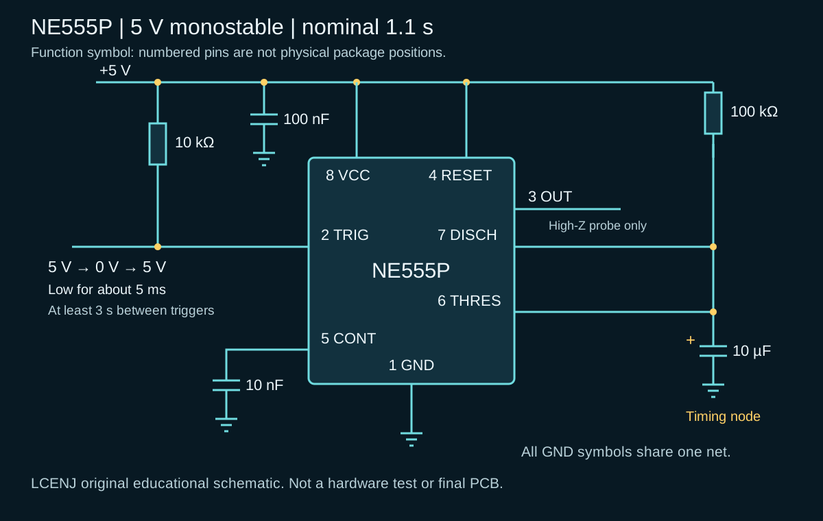
Wire the circuit with the supply off and check continuity across the breadboard rails. Confirm supply polarity and capacitor orientation before power-up. Your oscilloscope or logic analyzer must tolerate the signal voltage. Do not connect a 3.3 V-only instrument input directly to a nominal 5 V output.
Calculate pulse width and understand component tolerance
For an ideal capacitor starting at zero, the charging equation is VC(t) = VCC × (1 − exp(−t/RC)). Setting VC = 2VCC/3 gives t = RC × ln(3) ≈ 1.1RC. Enter resistance in ohms and capacitance in farads. Confusing microfarads with nanofarads changes the calculated interval by a factor of a thousand.
| R | C | Approximate time using 1.1RC |
|---|---|---|
| 100 kΩ | 1 µF | 0.110 s |
| 100 kΩ | 4.7 µF | 0.517 s |
| 100 kΩ | 10 µF | 1.100 s |
Considering only a ±5% resistor and a ±20% capacitor, the last example spans approximately 1.1 × 0.95 × 0.80 = 0.836 s to 1.1 × 1.05 × 1.20 = 1.386 s. This calculation includes only the assumed R and C tolerances. It excludes threshold variation, leakage, temperature and residual capacitor voltage; it is not a guaranteed circuit timing range.
In the ideal model, the threshold scales with supply voltage and VCC cancels from the timing equation. A noisy real supply is a different situation. If precise timing matters, first specify the required error and capacitor characteristics, then consider measurement, calibration or a digital timer.
Common NE555 wiring and timing mistakes
- Holding the trigger low: a grounded TRIG input is not a momentary command. It must return high in time for the pulse to finish normally; the NE555 datasheet requires at least 10 µs before the timing interval ends. A mechanical switch can also bounce, so pressing a button does not guarantee a clean trigger.
- Leaving RESET floating: tie it to the supply in this simple circuit. A separately controlled reset needs a valid logic level.
- Choosing the wrong capacitor: reversed polarity, leakage or a different actual capacitance can move the result away from the calculation. Extremely large R and C values are not a reliable shortcut to long intervals.
- Treating the output as an ideal supply: its high voltage changes with load and need not equal VCC. Motors and relays require an appropriate driver stage and inductive-load protection. A headline output-current rating does not qualify a complete driver design.
- Substituting any chip called 555: the bipolar TI NE555 has a recommended 4.5–16 V supply range; do not select it for a 3.3 V rail. A CMOS device such as TS555 has different conditions. Read its separate ST datasheet rather than assuming identical limits.
For a microcontroller interface, continue with 3.3 V and 5 V logic-level conversion. For recommended operating conditions versus absolute limits, see how to read an electronics datasheet.
Check the circuit one observation at a time
- In the waiting state, verify the 5 V rail and high levels at RESET and TRIG.
- Observe TRIG, the capacitor node and OUT during the same cycle. The output alone cannot explain the failure mechanism.
- Apply a short trigger and check the output transition and capacitor charge. After the interval, the capacitor should discharge again. Allow recovery before the next trigger.
- Record measured pulse width, actual R and C values, supply voltage and device type. Use those observations to investigate a timing error before replacing the IC.
This is an educational analysis and calculation. LCENJ has not physically tested this circuit. The accompanying validation checks the RC arithmetic, tolerance example and publication package only.
NE555 frequently asked questions
Does timing automatically start when power is applied?
This connection starts a timing interval from a valid trigger. Do not equate its uncontrolled power-up transient with a deliberately designed power-on delay circuit.
Does a larger capacitor always produce a longer interval?
It does in the ideal RC model, but capacitor leakage and characteristics affect the real circuit. A larger value does not automatically make timing more reliable.
Are NE555P and NE555D the same package?
In TI's ordering scheme, P denotes PDIP-8 and D denotes SOIC-8. Their mounting and footprint differ; check the complete ordering code.
Sources and editorial method
- TI NE555 datasheet SLFS022K, March 2026: pinout, operating conditions, triggering and one-shot connection.
- TI LM555 timing reference; its specifications do not replace the NE555P specifications.
- ST TS555 CMOS datasheet for the family comparison.
Sources and purchase links checked on 15 October 2026. Original text and schematic were prepared with AI assistance and reviewed against official references. Worked examples are calculations, not measurements or final-product qualification.
Question and answer article
Ask your technical question
Questions and answers are published after moderation. Authors can see their own pending drafts.
No confirmed questions have been registered for this article yet.