NAU7802 Qwiic Scale: an I2C bridge interface and trustworthy readings
Follow SparkFun’s circuit from bridge excitation and differential inputs to I2C, PCB routing and library fault reporting, with worked calculations and explicit limits.
Contents
SparkFun’s Qwiic Scale connects a load cell to a microcontroller. A load cell produces a very small differential voltage when loaded; the board amplifies and digitizes it so that a host can read the result over I2C. That number is not yet a mass in grams: calibration is still required. We will follow the measurement path from the load-cell supply to valid data acquisition, examining why bridge current, regulator operation and communication-error reporting matter as much as the wiring.
This review examines SparkFun’s Qwiic_Scale at ab136d756a78, April 11, 2019, using its schematic, PCB and component records. The companion library is a separate repository and revision, identified below. Worked numbers are hypothetical calculations.
The complete board and the bare chip
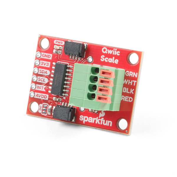
The assembled design is SparkFun SEN-15242 with spring terminals; it also needs a load cell and a host. On November 11, 2026, the seller’s page contained both “In stock” and “Backorder”, so its text did not establish unambiguous availability. The SO16 NAU7802 used in the circuit is a bare IC, not this complete board. An exact matching Iranian seller and availability were not verified. An HX711 module is not a direct replacement for this board’s I2C interface.
What this architecture simplifies
A four-wire full-bridge load cell has two excitation connections and two signal connections. Excitation supplies the bridge; mechanical deformation produces a small difference between its output voltages. The programmable-gain amplifier, or PGA, amplifies that difference. The analog-to-digital converter, or ADC, turns it into raw counts. The host must convert counts into grams using a reference mass.
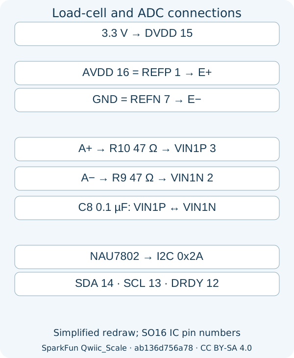
Unlike OpenScale, which includes a processor and USB, this board mainly supplies the acquisition stage. Its NAU7802 uses I2C with a fixed seven-bit address, 0x2A. The two Qwiic connectors share SDA, SCL, ground and power; they are not independent buses. Simply chaining two same-address boards does not resolve their conflict. A bus separator such as an I2C multiplexer needs evaluation against the system’s electrical and software conditions. For basic mounting and calibration practice, start with the load-cell and HX711 tutorial.
Bridge excitation: a small limit with large consequences
To understand the supply’s effect on the measurement, follow both bridge excitation and the converter reference. The 3.3 V input reaches DVDD, the digital supply on pin 15. Internal regulator output AVDD on pin 16 supplies positive bridge excitation and also connects to REFP, the ADC’s positive reference on pin 1. Negative excitation and REFN on pin 7 connect to ground. The converter measures the bridge signal relative to its reference. Because both depend on excitation, some common supply variation can cancel in the ratio. This ratiometric arrangement does not eliminate cable drop, input saturation or interference that changes only one path.
The internal supply is an LDO: a linear regulator designed to operate with a relatively small input-to-output voltage difference. The required difference is still not zero. Nuvoton’s Rev 2.6 datasheet, page 4, specifies 0.3 V of DVDD headroom for this output and a 10 mA load-current limit. The reviewed library initially selects a 3.3 V output. If DVDD is itself only 3.3 V, writing that setting does not provide the required headroom or establish that the output actually reaches 3.3 V. The voltage must be checked under load.
Nuvoton’s Rev 2.6 datasheet, page 4
Assume excitation is actually 3.0 V and the bridge input resistance is 350 Ω. Bridge current is approximately 3 / 350 = 8.57 mA, and power is 3² / 350 = 25.7 mW. That load approaches the stated limit; other AVDD loads and real operating variation need separate accounting. A 120 Ω bridge would require 25 mA under the same assumption, exceeding that limit. For a hypothetical 2 mV/V load cell, full-scale output at 3 V excitation is 6 mV. These assumptions are not specifications for every load cell.
One option is to evaluate a lower excitation voltage that the supply and load-cell specifications permit while leaving sufficient regulator headroom. The tradeoff is a smaller bridge signal, and mass calibration must be repeated after the change. An external bridge supply requires the reference connection, input-voltage limits and isolation of the internal regulator output to be reconsidered; it should not be treated as a one-wire substitution. Include bridge and power-indicator current alongside the IC’s own current when estimating consumption. The IC standby figure is not the whole system’s standby consumption.
The analog input and its actual filter
Schematic terminal J7 assigns pin 1 to positive excitation, pin 2 to ground, pin 3 to A− and pin 4 to A+. Each connection has two physical pads. Identify pin 1 from the actual board and CAD rather than inferring orientation from a photograph. Load-cell wire colours are not universal. A+ passes through R10 and A− through R9, each 47 Ω, to VIN1P pin 3 and VIN1N pin 2. C8, 0.1 µF, connects between the two inputs, not from each input to ground.
The two 47 Ω resistors and the capacitor between the inputs form a differential filter: they act on the voltage difference between A+ and A−. Temporarily ignoring bridge source resistance gives a pole frequency of approximately 1 / [2π × (47 + 47) × 0.1 µF] ≈ 16.9 kHz. This describes that analog filter stage; it is insufficient to establish 50 Hz rejection or output-data bandwidth at 80 samples/s. The ADC’s internal filter needs separate analysis. The second channel already includes C11, a 330 pF capacitor, and closed jumper J1CAP. Library initialization also enables PGA_CAP_EN.
sampling and aliasing lesson
Bus loading, PCB and assembly
R2 and R3 are 2.2 kΩ pull-ups connected to 3.3 V through JP3. A pull-up returns an idle communication line high; a device driving the line low must conduct its current to ground. Two identical pairs on parallel-connected boards give an equivalent 1.1 kΩ per line. Assuming a near-zero low level, the current is approximately 3 mA. Adding boards therefore requires the equivalent resistance, cable capacitance and every device’s current-sinking capability to be checked again. Use a compatible 3.3 V interface for this Qwiic board: a correct address alone does not establish voltage compatibility.
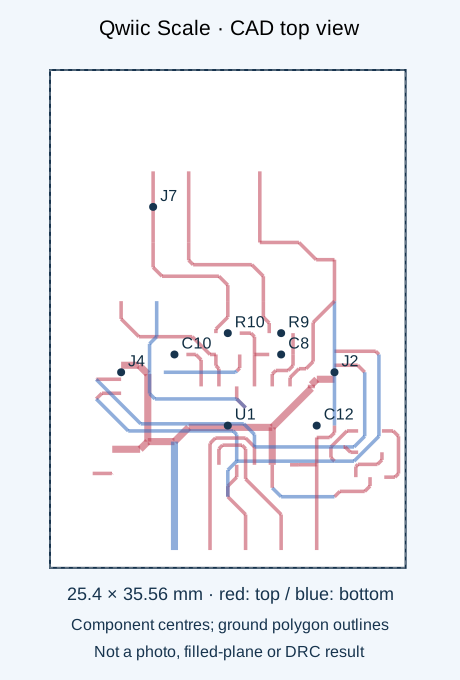
The design measures 25.4 × 35.56 mm and includes ground polygons on both copper layers. The short input routes after the resistors appear on the top layer at 0.254 mm width. Those observations do not establish precise matching, impedance or measurement accuracy. Provide cable strain relief rather than transmitting cable pull to the terminal and PCB. The mechanical load must pass through the load-cell structure. For a long cable near a motor, proposed input protection and shielding require checks of leakage, capacitance and noise introduced by the protection device; adding a TVS does not guarantee an improvement.
From library startup to a valid reading
The separately reviewed companion software is SparkFun’s library at e15210f5b58f, version 1.0.6. It is not presented as firmware contained in the 2019 hardware snapshot. Its begin function checks acknowledgement, initializes power and analog settings, selects gain 128 and 80 samples/s, and calibrates the analog front end. AFE calibration addresses the electronics; it does not replace calibration with a reference mass.
After initialization, the application must wait for a fresh conversion. The available function reads the conversion-ready bit; asking for that status more often does not increase the sample-production rate. By default, getWeight averages eight readings with a 1000 ms timeout. At the nominal 80 samples/s setting, conversions are spaced 12.5 ms apart, so eight conversions represent roughly 100 ms of collection time. Startup, settling and application execution add to that time.
In this software revision, some failures are not distinguishable from valid measurements. getAverage returns zero when its timeout expires. get24BitRegister also returns zero after a failed acknowledgement, or ACK, and checks only that at least one byte is available before making three byte reads; it does not verify receipt of all three. Another path in getRegister returns a negative error through the unsigned uint8_t type, while getBit carries no separate error status. An application that receives only the final number may therefore confuse a failure with a legitimate zero. This limitation was identified by reading the code; its occurrence on a board was not tested.
A specific improvement would return a record containing status, counts and time: validate acknowledgement and exactly three received bytes, distinguish timeout from legitimate zero, and store tare or calibration only after valid acquisition. The cost is an interface change and additional fault handling in the host. Proposed validation should separately inject disconnection, one- and two-byte responses, valid zero and delayed readiness. Rejecting every zero is not a correct solution. Signed readings also help diagnosis: getWeight with its default allowNegative=false clamps readings below the offset to zero.
Bring-up and evaluating the result
With power disconnected, check pin assignments and the full-bridge wiring. Connect a suitable 3.3 V host and common ground, then measure DVDD and excitation under bridge load. After discovering the address, check initialization and internal-calibration success. Inspect raw readings and fault status first; tare an empty, stable platform and then apply a known mass. In a synthetic example, an empty reading of 100000 and a 160000 reading under 500 g give 120 counts/g. A later 130000 reading corresponds to 250 g. Interpret the factor’s sign against actual signal polarity.
After calibration, record other reference masses, return to zero, repeated loading, load-position effects and warm-up separately. A 24-bit output does not guarantee 24-bit mass accuracy. The repository provides Eagle files, but no Gerber files appeared in the reviewed tree. Manufacture requires completed component specifications, manufacturing outputs and independent checks.
Sources: the pinned schematic, PCB and historical Rev 1.7 datasheet bundled with the design, alongside Nuvoton’s current datasheet and the separately pinned library. Hardware and adapted drawings use CC BY-SA 4.0; the original notice and separate software licence are retained. Compare the processor-equipped architecture in the OpenScale review.
Question and answer article
Ask your technical question
Questions and answers are published after moderation. Authors can see their own pending drafts.
No confirmed questions have been registered for this article yet.