CAP1203 touch board review: from electrodes to I2C events
Follow SparkFun’s pinned touch-board schematic and PCB through power, pull-ups, electrode geometry and blocking swipe behavior in the companion library.
Contents
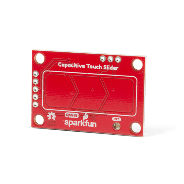
SparkFun’s CAP1203 board provides touch buttons and simple finger-gesture detection. It has three copper sensing areas; the IC detects which area is touched, and a separate microcontroller reads the result through the two-wire I2C interface. Tracking the order in which these areas are touched can identify a swipe, but the board does not measure a precise finger coordinate in millimetres. We will follow the signal from the electrodes and power circuitry to the code that reads touch events, examining how copper geometry, the cover, grounding and firmware affect the result.
This review reads the schematic and PCB in SparkFun's hardware repository at a78a8703b50e, committed on May 31, 2019. The separate SparkFun library is reviewed at 8548d0a082c8, committed on May 9, 2021, with version 1.0.5. These are separate repositories and revisions. The review date is November 12, 2026; commit age alone establishes neither product quality nor novelty.
Identify the board before sourcing it
The reviewed board is SparkFun SEN-15344. U2 has the CAD value “CAP1203” and footprint SO08-TIGHT; that abbreviated value does not prove the assembled chip's full ordering suffix. For comparison, CAP1203-1-SN is a bare SOIC-8 device, distinct from the board. The manufacturer's direct SEN-15344 page displayed both “In stock” and “Backorder” today, so definite availability was not established. An Iranian product page with a verifiable exact model and package was not found in the regional search; no local link or stock claim is invented.
From a touch to a status bit
Each copper area is an electrode: a conductive surface connected to a sensing input. Bringing a finger near it changes the capacitance seen at that input. The IC evaluates the change against a reference level, called the baseline, and decides whether each channel is touched. Capacitance is measured in farads, but the touch-status output is not a capacitance reading in farads or a measurement of finger pressure; it reports the result of the touch decision.
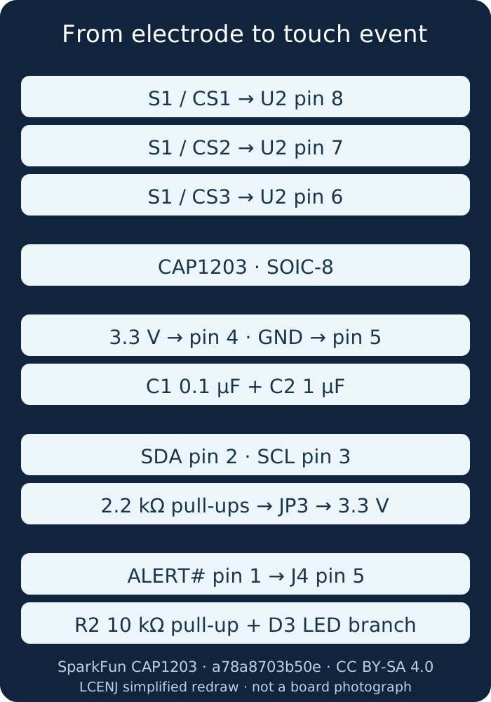
CS1 connects U2 pad 8 to S1 pad 1 and J3 pad 1. CS2 connects U2 pad 7 to the second pads; CS3 connects U2 pad 6 to the third pads. S1 is the three-part copper sensing pattern. J3 exposes those same sensitive inputs, rather than an independent digital interface. Longer wiring or external electrodes change baseline capacitance and noise pickup; they require retuning and testing.
A channel sequence can be classified as a rightward swipe. That differs from continuously measuring position. For rulers, encoders or accurate coordinates, the position-sensor and encoder lesson addresses a different requirement.
Power: IC current is not board current
Start the supply analysis with the net labelled 3.3V in the schematic. It connects J1, J2 and J4 to U2 pin 4, VDD; pin 5 connects to ground. C1, rated 0.1 µF, and C2, rated 1 µF, connect between this supply net and ground. This revision shows no regulator, logic-level translator or dedicated input-protection stage in the Qwiic supply path. Applying 5 V to a connector will therefore not automatically produce a regulated 3.3 V supply.
Microchip's DS00001572B datasheet (same document hosted by SparkFun) specifies a 3–5.5 V operating supply for the IC. This does not authorize changing the voltage of a whole Qwiic network. Here, a compatible 3.3 V board and host connection is assumed. Tolerance of some digital pins must not be extended to CS inputs or another host.
The power-indicator branch contains R3=1 kΩ and red LED D2. Assuming a 1.9 V LED drop, its current is (3.3−1.9)/1000=1.4 mA. This is calculated, not measured. The IC's typical active current under the datasheet table's conditions is about 0.5 mA. Consequently, the IC's Deep Sleep figure cannot represent the board: indicators, pull-ups and the host also consume power.
I2C, pull-ups and interrupts
SDA reaches U2 pin 2 and SCL pin 3. J1 and J2 connect to the same nets; the second connector is not a separate bus. The reviewed library defines seven-bit address 0x28, and this schematic has no address-selection jumper. Decide how to separate same-address devices before connecting several boards.
I2C lines need pull-up resistors to return them to a logic-high level. Here R5 connects SDA to the supply and R4 does the same for SCL; both are 2.2 kΩ. They share jumper JP3, whose narrow copper bridge connects them by default. When a device drives a line low, it must conduct the pull-up current to ground. Assuming a 0.4 V low level, each low line draws approximately (3.3−0.4)/2200 ≈ 1.32 mA. Four boards with identical pull-ups in parallel reduce the equivalent resistance to 550 Ω, raising the current to approximately 5.27 mA per low line. When chaining boards, check every participating device’s current-sinking capability as well as cable capacitance and signal rise time; a second connector alone does not establish compatibility.
The IC can signal an event to the host through ALERT# on pin 1. This output is active-low: its voltage goes low when asserted. In the schematic the signal is named !INT and reaches J4 pad 5. The 10 kΩ resistor R2 pulls it up through JP1. A separate branch connects the supply through JP2, the 1 kΩ resistor R1 and green LED D3 to the same signal, providing an event indicator. Opening JP1 disconnects the resistor pull-up branch, whereas opening JP2 disconnects the LED branch. With an assumed 2.1 V LED drop and 0.2 V output-low level, the indicator draws about 1 mA. Its consumption can therefore be evaluated separately; removing the indicator does not remove the independent pull-up resistor.
What the PCB reveals
The design file defines a 38.1 × 25.4 mm board. U2 and the two supply capacitors are placed near one another: U2 is centred at (17.78, 12.7) mm, C2 at (21.336, 12.7) mm and C1 at (22.86, 12.7) mm. Placing supply capacitors near the IC is intended to shorten the path for transient current. Centre-to-centre distances alone, however, are insufficient: follow the copper from the supply pin to the capacitor and the return path through ground. Without examining that loop, placement does not establish its inductance or the capacitors’ effectiveness.
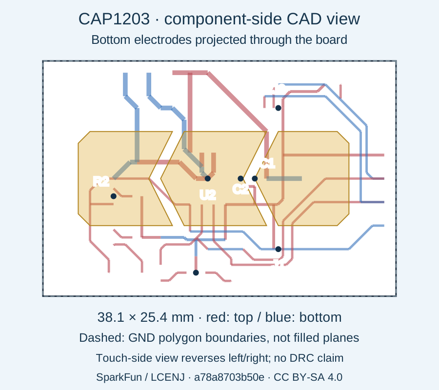
S1 has placement rotation MR0, putting it on the opposite board side. Left and right in this component-side view therefore differ from looking at the touch surface. This matters when interpreting Left and Right software names. Interleaved electrode shapes provide overlapping contact regions during finger movement; multiple channel detections still do not establish an accurate position output.
Ground copper areas, or polygons, are defined on both PCB layers with a design isolation setting of 0.3048 mm. This is a setting in the CAD file: viewing a polygon boundary does not establish every clearance after copper filling or prove manufacturing acceptance. In the application, keep CS input routes and J3 wiring away from switching paths, motor cables and paths carrying changing LED currents to reduce noise pickup. Suitable spacing and layer arrangement depend on the device’s operating environment.
What the library does—and where to take care
begin checks the addressed device's response and compares its product ID with 0x6D, then selects 2X sensitivity, enables interrupts and clears interrupt status. Adjustable sensitivity is already a project feature. Covers, moisture, gloves and external electrodes can change the required sensitivity and thresholds; the default does not guarantee operation in every condition.
In the pinned SparkFun_CAP1203.cpp, readRegister returns zero when no byte is available and does not expose endTransmission status to its caller. A status-returning function therefore has no separate transfer-error return. A false touch result alone cannot prove healthy communication and an absent finger. This is an interface limitation visible in that commit, not a reported hardware failure.
The functions isRightSwipePulled and isLeftSwipePulled use 100 ms windows for parts of gesture detection. Inside them, however, a loop waits for the finger to be released without imposing a time limit on that wait. If a channel continues to report a touch, the function can remain there and delay the application’s main loop. The 100 ms windows therefore do not guarantee a total execution time of 100 or 300 ms.
Two proposals, their costs and how to assess them
For a device that must also service communication or another control task, gesture detection could use a state machine. On each main-loop iteration, the program would read one valid channel status, remember how far the gesture has progressed and return control to the application. Recording each state’s start time would also allow the wait for finger release to time out. This avoids keeping execution inside a long blocking loop, but requires more states, defined simultaneous-touch behavior and timing-boundary tests. The proposed interface should report I2C transfer validity separately from touch status. This proposal has not been applied to the upstream library.
Assess the proposal using specified synthetic sequences and a controlled clock: left→middle→right, reverse direction, held finger, simultaneous touches, I2C loss and counter wrap. Then measure response and final-cover behavior on a real sample. These are proposed acceptance methods, not completed tests.
For battery use, evaluate disconnecting D3 through JP2 and choosing an appropriate power state. D2 is a separate power LED with no dedicated disconnect jumper visible here; changing it requires a separate hardware modification and assembly/current review. Measure whole-board current first. Lower consumption may cost a diagnostic indicator or alter wake timing. The IC's 5 µA Deep Sleep figure establishes neither product standby current nor touch detection: the datasheet says no sensor inputs are active in that state.
Bring-up and review limits
Before applying power, match revision, connector view, 3.3V/GND/SDA/SCL and jumper states against the same files. Initialize the host I2C interface using its documented pins, check begin and identification, then individual channels and gesture order. For false activation, investigate supply, grounding, cover, J3 wiring capacitance and baseline; higher sensitivity is not always a remedy. For missing responses, distinguish address, host-pin and parallel-pull-up issues from actual touches.
Hardware and derivative redraws use CC BY-SA 4.0. The hardware notice and library licence are provided. The library licence declares MIT; original headers also carry a beerware note. Original notices are retained. SparkFun owns the source project; this is LCENJ's editorial analysis.
Question and answer article
Ask your technical question
Questions and answers are published after moderation. Authors can see their own pending drafts.
No confirmed questions have been registered for this article yet.