MAX17043 Fuel Gauge Review: From Battery Voltage to a Useful Charge Estimate
Trace SparkFun’s pinned battery-gauge schematic and PCB through two filters, I2C pull-ups, charge estimation and invalid-read handling.
Contents
SparkFun's MAX17043 board measures the voltage of a single lithium-ion cell and uses the IC's battery model to estimate remaining charge. A separate microcontroller reads both values over I2C. The central distinction is that measured voltage, estimated charge percentage and remaining operating time are different quantities. The board alone is neither a battery charger nor a protection circuit.
We will trace the battery input through the schematic and PCB, then examine how the program reads the result and how a communication failure can resemble “zero charge.” The aim is a dependable battery report for a portable device.
The board, revision and sourcing
The hardware reference is SparkFun's original repository at commit e3e707c39049, dated 27 February 2023. The board file carries the text v12; the README identifies v1.2 as TOL-20680. U2 is named MAX1704X in CAD with a TDFN-8 package. The MAX17043 identity comes from the same product's documentation; the abbreviated CAD value alone does not establish an exact IC ordering suffix.
For the complete board, SparkFun's direct TOL-20680 page displayed “In stock” on 15 November 2026. Analog Devices' MAX17043 page provides bare-IC and package information; the bare IC and assembled board are different purchases.
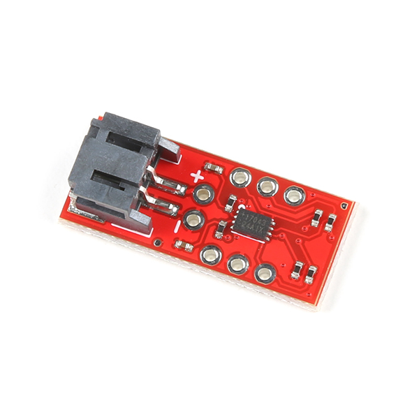
Where does the percentage come from?
A discharging battery does not maintain a fixed terminal voltage. A heavy load can pull its voltage down, with some recovery after the load eases. Temperature, chemistry and battery condition also matter. A linear rule such as “3 V is empty and 4.2 V is full” is therefore unsuitable as a universal conversion for every cell and load.
The MAX17043 measures voltage with an analogue-to-digital converter, while its ModelGauge algorithm estimates relative state of charge, or SOC, from battery behaviour. This architecture does not use an external current-sense shunt for charge counting, helping keep the sensing path small and low-loss. The suitability of the battery model remains important. The IC is not a general current meter or a battery-capacity tester reporting measured milliamp-hours.
A device that shuts down at a particular voltage may be unable to use all the residual energy considered by the battery model. Thus 20% should not be translated into 20 minutes, or 20% of the nameplate capacity deliverable at a USB output. The distinction between nominal and delivered energy is covered separately in the mAh and Wh guide.
Two supply inputs with different jobs
In this revision's schematic, the positive battery contact at JP1 and positive output at JP5 share V_BATT. That path connects the battery to the application. Two separate branches feed the gauge:
- R1 = 1 kΩ and C1 = 1 µF filter the CELL measurement input at U2 pin 2.
- R2 = 100 Ω and C2 = 10 nF feed the IC supply, VDD, at pin 3.
- CTG at pin 1, GND at pin 4 and the exposed pad EP connect to ground. Both filter capacitors return to that same ground.
Resistance is expressed in ohms and capacitance in farads; a microfarad is one millionth of a farad and a nanofarad is one billionth. These are resistor–capacitor filters, not a voltage divider that converts a two-cell pack into a one-cell input. In an ideal unloaded model, their RC time constants are 1 ms for CELL and 1 µs for VDD. Those calculations do not specify the IC's register-update rate or replace real noise measurements. This board's documented battery application is single-cell; a higher-voltage series pack is not a direct substitute. In the diagram below, the numbers identify pins; symbol positions do not show the IC's physical pin arrangement.
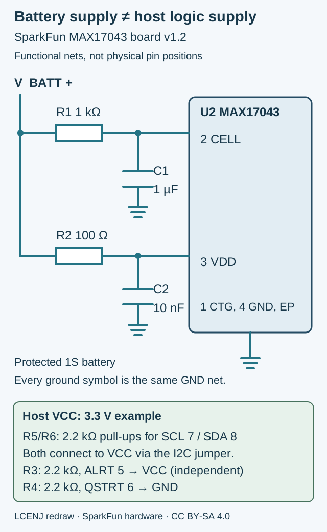
The board pin labelled VCC is different from both the battery input and the IC's VDD. VCC supplies the SDA, SCL and alert pull-up resistors so their logic-high level can match the host. For a 3.3 V host, regulated 3.3 V at VCC with a common ground is a straightforward starting point. The IC's own specified supply range is 2.5–4.5 V. Do not confuse that range with the digital-pin limits or feed battery voltage into an MCU supply input without checking the host design.
I2C and the three 2.2 kΩ pull-ups
U2 pin 7, SCL, and pin 8, SDA, connect to the correspondingly labelled board pads. The gauge's seven-bit address is 0x36. The values 0x6C and 0x6D include the write or read bit as transmitted on the bus. Use 0x36 with an API expecting a seven-bit address. For background, see the interface comparison.
R5 and R6 are the clock and data pull-ups, each 2.2 kΩ. The three-pad jumper named I2C connects them to VCC by default. Opening it removes those pull-ups; it does not change the device address. Pull-ups on other boards appear in parallel. Assuming a 3.3 V rail and a 0.4 V low level, one resistor requires approximately (3.3 − 0.4) / 2200 = 1.32 mA of sink current. A second identical pull-up approximately doubles that current. Device current-sinking capability, cable capacitance and signal rise time must be checked together.
R3 is the independent pull-up for the active-low ALRT output at pin 5, abbreviated ALT on the board. Opening the I2C jumper does not remove this separate resistor. Pin 6, QSTRT, is labelled QST; R4 pulls it down through 2.2 kΩ. A rising edge restarts the estimate. This input is different from the alert output.
Disabling pull-ups also does not make two same-address MAX17043 boards independently addressable. Such a system needs bus separation or another suitable arrangement; the I2C multiplexer review examines that separate problem.
What the PCB reveals
The board outline is 10.16 by 24.13 mm. Two three-pad rows, the battery connector and positive/negative output pads occupy that small area, with no separate mounting holes visible in the design. Match the viewing direction when reading the underside: left and right in a bottom-view photograph are not an IC top-view pin diagram.
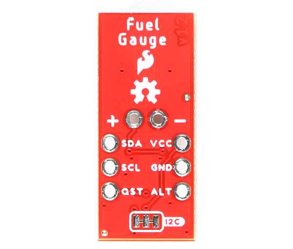
The battery-positive path between connector and output includes 0.4064 mm traces; its filter branches use 0.2032 mm routes. These are file dimensions, not a board-current rating. Copper thickness, permitted temperature rise and installation conditions would also be needed. Keep application load current out of the sensitive CELL branch, and do not treat R1 or R2 as the application's series load resistor.
Ground polygons are defined on both layers with 0.2032 mm isolation settings and interlayer ground vias. Polygon boundaries alone do not establish the final poured-copper geometry or manufacturing acceptance. For a derivative layout, follow the VDD–C2–GND and CELL–C1–GND loops in the poured design and keep pulsed load returns away from the measurement reference. A common ground is necessary, but a shared high-drop return can still corrupt a reading.
The reviewed schematic contains no charger, battery-protection switch or fuse. Those functions must be provided appropriately by the battery and host system. The gauge itself also consumes battery energy: the datasheet's 50 µA typical active-IC current is not the complete device's consumption. Holding that illustrative current constant gives about 1.2 mAh per day. A battery-life estimate must also include the pull-ups, host and load pattern.
Turning register bytes into volts and percent
A register holds a value or setting inside the IC that the host can read or change as specified. The MAX17043 VCELL register at 0x02–0x03 contains a 12-bit measurement in the upper bits of a two-byte word. For a fully hypothetical example, bytes 0xC8 and 0x00 form 0xC800. Shifting right by four gives 3200 counts. At 1.25 mV per count, the calculated voltage is 4 V.
The SOC register at 0x04–0x05 uses the high byte for whole percent and the low byte for fractions in steps of 1/256%. Hypothetical bytes 0x32 and 0x80 give 50 + 128 / 256 = 50.5%. That numerical step does not establish approximately 0.004% accuracy of actual battery charge. See the calibration lesson for the distinction between resolution and accuracy.
VCELL has its own initial conversion period and updates every 500 ms during normal operation. Reading SOC from the host also does not necessarily cause a new estimate. Faster I2C polling cannot create fresh measurements by itself. Store the reading time, communication validity and sample freshness alongside the value.
Firmware behaviour and a concrete limitation
The hardware repository's combined Arduino example initializes Wire, the gauge and the OLED. It stops in a loop if gauge or display initialization fails. It then performs one quick-start, sets a 20% alert threshold and repeatedly reads voltage and SOC, clears the alert, reads alert status again, and updates OLED and Serial output. A 500 ms delay follows; the full cycle is longer because reading and display work also take time.
To establish the API behaviour, we separately reviewed SparkFun's library at commit 6ea1765a513d, dated 1 September 2023, version 1.0.4. This is a different repository and revision from the board. Its getVoltage and getSOC methods implement the conversions above. The older C example in another folder targets hardware v10 and an 8 MHz ATmega328, a different hardware revision and platform from this board’s Arduino example.
One specific limitation is visible in the pinned library: read16 retries up to three times when it does not receive two bytes, but returns its initial zero value if all attempts fail. getSOC converts that zero into 0%. A zero result alone therefore does not establish an empty battery. In version 1.0.4, the failed-read path is not distinguished from the initial zero value.
Clearing the alert before reading it, as the combined example does, also does not preserve the pre-clear state for reporting. An event logger should first read and retain valid status, then clear it according to its policy. Quick-start is not a general calibration or a cure for every unexpected result: it restarts the estimate from current conditions and should not be triggered without reason on every loop.
Proposed improvement: return validity with the value
For a battery-powered product, our proposed improvement is to separate transaction success from the returned value. The reading layer should report whether both bytes arrived successfully. The presentation layer should decode only valid data and explicitly show an invalid or stale sample on failure. Treating every zero as an error would also be incorrect because 0% can be a genuine reading.
The benefit is avoiding a decision based on a fabricated zero. The cost is an API change and error-state handling by its callers. Evaluate it by separately injecting zero-, one- and two-byte responses and address-write errors; only a valid two-byte result should reach the conversion. Three library retries do not establish a strict response deadline: the selected platform's Wire calls also need bounded, verified waiting. This is a proposed change, separate from the library’s current behaviour.
A replacement IC likewise needs more than a similar name. Other family members use different voltage formats and features; the reviewed library itself has separate conversion branches for the 17043 and 17048. Check package, pins, battery model and software support before substitution.
Bring-up and evaluation
- With power and battery disconnected, verify connector polarity against the board markings. Similar JST connectors do not guarantee identical cable polarity. Check ground continuity and shorts.
- Select a suitable 3.3 V I2C host and a protected single-cell battery. Connect common ground, board VCC to the host logic rail and SDA/SCL to that host's documented pins. The application's VBATT input must tolerate the battery voltage; this board does not provide a regulated 3.3 V output.
- After applying power, check battery voltage and both sides of the supply filter with suitable instruments. Verify communication at 0x36 and complete two-byte reads before reporting voltage and SOC. Test threshold configuration, alert recording and clearing separately before relying on the warning.
- Compare reported voltage with a suitable reference at the same point. For SOC evaluation, log the specified battery under the real load pattern and within its permitted operating limits, recording temperature, device cutoff and transient loads. Agreement at a few voltage points alone does not validate charge-percentage accuracy.
The architecture is simple and useful for reporting charge in a small portable device: voltage sensing and battery modelling reside on the board, while application decisions belong to the host. Reliable reporting still depends on wiring, battery selection, valid samples and system evaluation.
Sources and licences
The pinned schematic and PCB belong to SparkFun Electronics and are licensed CC BY-SA 4.0. Photographs come from its official guide under the same licence. The power-path drawing is an LCENJ adaptation of that schematic.
IC specifications and registers were checked against the original MAX17043/MAX17044 document, 19-4811, Rev 7, January 2017. SparkFun's store links an older Rev 3 PDF; it is not the numerical reference for this article. The reviewed library is MIT licensed; the hardware repository's code notices differ by file and are kept separately in the licence notes. Sources were reviewed on 15 November 2026.
Question and answer article
Ask your technical question
Questions and answers are published after moderation. Authors can see their own pending drafts.
No confirmed questions have been registered for this article yet.