SparkFun AP63203 buck supply: capacitors, inductor and PCB review
Follow the SparkFun 3.3 V buck from DC input to output: capacitors, inductance, EN control, power loss, PCB current paths and a practical bring-up plan.
Contents
SparkFun's Buck Regulator board uses an AP63203 to reduce a DC supply to a fixed 3.3 V output. Its educational value lies in the small power circuit: an input capacitor, two internal MOSFETs, an inductor and output capacitors cooperate to supply a load. The “2 A” rating alone does not establish usable current under every temperature and installation condition.
Imagine a 3.3 V digital circuit and a 12 V workshop supply. A direct connection exposes the circuit to the wrong voltage, while a linear regulator would turn the voltage difference into substantial heat at a one-ampere load. We follow SparkFun's design from energy conversion to the checks needed before connecting a valuable load.
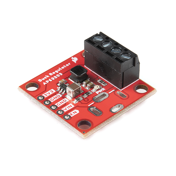
Which project and board are being reviewed?
The design belongs to SparkFun's Buck_Regulator_AP63203 repository. We examined commit 63cdc8eadd1258e32630f4e8ce2c1978d6ed62a5, dated August 5, 2021, on November 9, 2026. The schematic and PCB discussion concerns only the larger board in SparkFun Buck Regulator - AP63203/Hardware. The repository also contains BabyBuck; we do not attribute its wiring or layout to this board.
Selecting the board and component
The corresponding assembled product is SparkFun COM-18356, shown as in stock on its manufacturer's page on November 9, 2026. For a custom build, check AP63203 and the TSOT26 pin assignment on Diodes Incorporated's product page. This project's library calls its footprint SOT23-6; a similar package name or six leads does not establish that another chip is interchangeable. COM-18357 is the smaller BabyBuck and is a different mechanical choice.
Why use a switching power supply?
A buck converter produces a lower output through rapid switching and energy storage in an inductor. An inductor resists rapid current change, while a capacitor stores electric charge; together they smooth the delivered output. The chip's specified input range is 3.8–32 V; near the upper limit, cable-induced voltage overshoot must also be considered. This board is not isolated: input and output share ground. Its input is DC; direct mains connection is outside this analysis.
At an assumed 3.3 V, 1 A output, load power is 3.3 W. A linear regulator from 12 V would dissipate approximately (12−3.3)×1 = 8.7 W. If we assume 90% buck efficiency solely for an example, input power becomes about 3.67 W, loss 0.37 W and average input current 0.306 A. These are not measurements of this board. They explain why output current, input current and linear-regulator heating are different quantities.
Follow the schematic's energy path
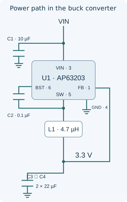
In the schematic at this commit, chip pin 3 connects to VIN and pin 4 to GND. C1 is 10 µF, described by its library device as a 1210, 50 V component, between input and ground. It supplies some of the pulsed current near the converter. Replacing it with a capacitor far from the board does not preserve the same high-frequency current path.
The AP63203 contains both switching MOSFETs, so the absence of a separate power diode is consistent with a synchronous buck. SW pin 5 connects to L1 and one end of C2. L1 is 4.7 µH; its other end creates the 3.3 V output net. C3 and C4, each 22 µF, connect that output to ground. FB pin 1 directly senses the output. This is a fixed-output device: R1 and R2 do not adjust its output voltage.
C2 is 0.1 µF between BST pin 6 and SW pin 5. This bootstrap capacitor supports the high-side MOSFET's drive; it is neither an input bypass nor an output capacitor. Connecting its second terminal to ground instead of SW would materially change this circuit.
EN, connectors and the output indicator
R1 and R2 are both 100 kΩ: R1 runs from VIN to EN, and R2 from EN to ground. Temporarily ignoring the pin's internal current, a 12 V input places EN near 6 V. Internal currents and hysteresis affect the actual switching thresholds, so that simple divider calculation is not an accurate UVLO design. More immediately, do not connect this board's EN directly to an unchecked 3.3 V GPIO. An open-drain output or transistor with suitable voltage tolerance can be evaluated for shutdown control, including the resistors and both powered and unpowered host states.
The following numbers are CAD pad numbers. Match the viewing side and actual board markings before wiring:
| Connection | Pad functions |
|---|---|
| J1, four-way terminal | 1: VIN; 2 and 3: GND; 4: 3.3 V output |
| J2, five-way header | 1: EN; 2: VIN; 3 and 4: GND; 5: 3.3 V output |
| J3, power-jack footprint | PWR pad to VIN and GND pad to ground; verify jack fit and polarity |
The input options join the same VIN net; they do not form an automatic multi-source selector. No separate input reverse-polarity protection is identified in this schematic. The chip's internal overcurrent or thermal protection does not replace polarity and cable-transient protection.
D1 receives output power through the 1 kΩ R3 and normally closed PWR jumper. Assuming a 2 V LED drop gives roughly 1.3 mA. Cutting the jumper disconnects the indicator, rather than shutting down the converter. Consequently the complete board's no-load current should not be equated with the IC's quiescent current. A glowing LED does not establish acceptable ripple, two-ampere capacity or a healthy load.
A worked inductor and capacitor example
For an ideal continuous-conduction estimate, assume 12 V input, 3.3 V output, 4.7 µH inductance and the nominal 1.1 MHz switching frequency. The switch's duty ratio is approximately 0.275. Using the inductor current slope gives the following result; enter inductance and frequency in henries and hertz:
D ≈ Vout / Vin = 0.275
ΔIL ≈ (Vin − Vout) × D / (L × f)
ΔIL ≈ 0.463 A peak-to-peak
Ipeak ≈ Iout + ΔIL/2
Ipeak at 1 A load ≈ 1.231 A
Peak current matters when selecting an inductor, but does not complete the selection. Consider tolerances, frequency, chip current limiting, temperature, winding resistance and saturation. The CAD provides 4.7 µH and a footprint, rather than independent evidence for a purchased inductor's saturation current or resistance. The current DS41326 datasheet, revision 3-2, November 2024 recommends 3.9 µH for AP63203. Its difference from the 2021 design alone does not prove a fault. Substituting L1 also cannot be called an assured improvement without checking load, loss and transient behavior.
C3 and C4 total 44 µF nominally. As a sensitivity example, suppose only this capacitance supplies an extra 0.5 A for 10 µs: ΔV = ΔI×Δt/C ≈ 0.114 V. This simplified model excludes the control loop, ESR and ceramic-capacitor DC-bias effects. It is not the board's measured voltage dip. The library describes 0603, 6.3 V output capacitors; the actual effective capacitance cannot be determined from the 22 µF label alone.
PCB review: follow current, not appearance
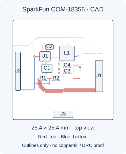
The PCB file defines a 25.4 × 25.4 mm outline. It contains ground polygon definitions on both layers and six GND vias. Top-layer VIN wire segments include widths near 0.81 and 1.02 mm. Width alone does not establish current capability: copper thickness, length, pad necks, temperature and the return path also matter.
SW is net N$5 in the CAD and uses a polygon to connect the switch, inductor and C2. Its fast voltage edges can couple into nearby circuitry; enlarging SW copper solely for cooling has a cost. Conversely, keep the loop through the input capacitor, internal switches and ground compact. Feedback should sense the intended output rather than an inappropriate high-current trace drop. The drawing below follows CAD coordinates and routes; final copper fills and DRC/CAM results have not been reconstructed.
Bring-up and improvements that can be evaluated
Before attaching a valuable circuit, inspect orientation, input polarity, shorts and solder joints. Start from a current-limited laboratory DC supply, for example at 5 V within this design's input range, choosing a limit suitable for the initial light-load test. Measure output with a multimeter, then add a known load in steps while recording voltage drop, input current and component temperatures. A multimeter shows an average; ripple and load transients require an oscilloscope and a short probe-ground connection. Our waveform-reading lesson develops that observation method.
For example, 33 Ω across 3.3 V draws about 100 mA and dissipates 0.33 W. Choose a suitable resistor power rating and thermal margin. That small test does not qualify two-ampere output. Raise load toward the actual requirement while checking temperature and oscillation; light-load and heavier-load timing behavior need not be identical.
For an installation with a long input cable, our proposed improvement is to evaluate polarity protection, a suitable fuse and transient suppression at the input. The benefit is reduced exposure to wiring errors and cable-induced surges; costs include voltage drop, board area and coordination with the supply and converter limits. Check a TVS's clamping voltage at the relevant current instead of choosing solely from its nominal voltage. Evaluate the change by measuring board input voltage and temperature under installation conditions. This proposed protection was not implemented or tested in the reviewed revision.
A second suggestion is to use the existing PWR jumper to compare no-load consumption with and without the indicator. That feature is already present; we are not proposing a missing jumper. A very-low-power redesign must also measure the EN resistor network and converter separately. For pulsed loads, investigate effective capacitance, current loops and startup response before simply adding a large capacitor: more capacitance can increase size and startup current.
This project needs no microcontroller or firmware to set its output. Adding demonstration code would not solve its power-design question. The CAD-extracted component list supports traceability rather than serving as a qualified purchasing BOM. Original SparkFun notices are retained in the upstream license file; the hardware and derived drawings are CC BY-SA 4.0. SparkFun owns the design; the proposals are LCENJ’s editorial analysis.
Question and answer article
Ask your technical question
Questions and answers are published after moderation. Authors can see their own pending drafts.
No confirmed questions have been registered for this article yet.