How source resistance causes ADC sampling errors
A correct divider output does not always produce a correct ADC reading. Follow the sampling capacitor, a worked calculation and three design options.
Contents
If a circuit produces the expected voltage but its analog-to-digital converter (ADC) reports the wrong value, excessive resistance in the circuit driving the input is one possible cause. In many ADCs, an internal capacitor must charge to the input voltage within a short sampling interval. A high source resistance slows that process. If the interval is too short, the converter digitizes a stored voltage that has not yet reached the actual input voltage.
We will follow a voltage-divider example to understand the problem: why might two circuits that both produce 3 V give different results when connected to an ADC? The numerical example uses a simple hypothetical model. We will then identify the specifications needed to apply the explanation to a real design.
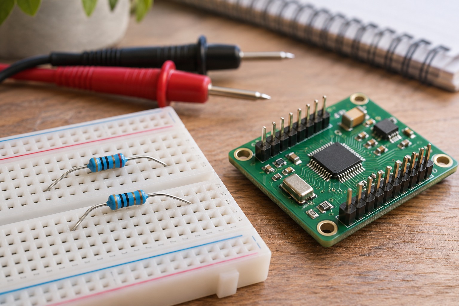
How does an ADC sample the input voltage?
An ADC converts a voltage into a digital number that a microcontroller can read. If a sensor has an analog output, this conversion is usually part of the measurement path. The sensor interface guide explains the distinction between analog and digital outputs.
Many successive-approximation, or SAR, converters connect the input to a sampling capacitor. The capacitor holds the voltage at a particular instant so that the converter can digitize it. An internal switch connects the capacitor to the input and then disconnects it; the connection is not permanent.
While the switch is closed, the external circuit charges the capacitor and its voltage approaches the input voltage. This interval is called the acquisition time. The switch then opens, and the ADC performs the conversion using the stored voltage. Acquisition time and conversion time are therefore separate parts of the process. Microchip's acquisition-time guide explains this distinction.
If the switch opens before the capacitor has charged sufficiently, the measurement already contains an error before conversion begins. A capacitor charging from zero toward 3 V will produce an underestimate in our example. If its previous voltage is above the new input voltage, the error can have the opposite sign.
Why do the divider's resistor values matter?
Suppose we want to halve an ideal 6 V supply using two equal resistors. The first resistor connects the supply to the output node, and the second connects that node to ground. If no current is drawn from the output, it will be 3 V whether the two resistors are 10 kΩ each or 100 kΩ each. One kilohm is one thousand ohms.
The input capacitor, however, needs current to charge. Two 100 kΩ resistors provide less charging current than two 10 kΩ resistors. The divider ratio alone therefore does not tell us whether the circuit is suitable: we also need to understand its behavior while the capacitor charges.
For the calculation, we can replace the divider, as seen by the ADC, with an equivalent voltage source and series resistance. This is its Thevenin equivalent. The equivalent voltage is 3 V. To find the equivalent resistance, replace the ideal voltage source with a short circuit; the two resistors are then in parallel when viewed from the output node. Two 100 kΩ resistors give an equivalent resistance of 50 kΩ. In the simplified model, this resistance limits the capacitor's charging current. TI's explanation of ADC source resistance uses the same equivalent circuit.
A calculation: two microseconds is not enough
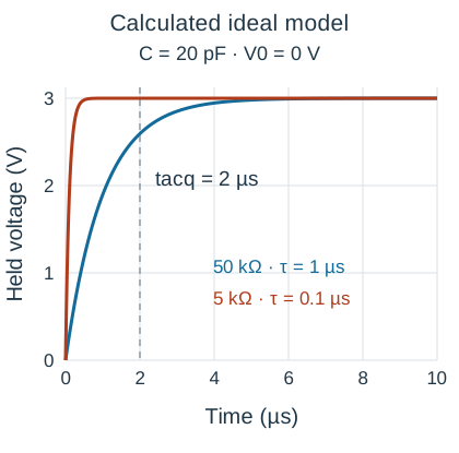
Assume a sampling capacitance of 20 pF. A picofarad is one trillionth of a farad, the unit of capacitance. Assume the capacitor initially holds 0 V and that the switch remains closed for 2 µs. A microsecond is one millionth of a second. For now, leave switch resistance, leakage and other capacitances out of the calculation.
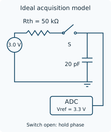
How quickly the capacitor approaches its final voltage depends on resistance multiplied by capacitance. We call this product the time constant and represent it by τ. Here, the time constant is one microsecond:
Rth = (100 kΩ × 100 kΩ) / (100 kΩ + 100 kΩ) = 50 kΩ
τ = Rth × C = 50,000 Ω × 20 × 10⁻¹² F = 1 µs
The time constant is not the time needed for a complete charge. After one time constant, a capacitor starting at zero has reached about 63% of its final voltage. Getting closer takes longer. In our ideal model, the expression below gives the capacitor voltage. V0 is its initial voltage, Vin is the final voltage, and t is the time for which the switch remains closed:
Vhold(t) = Vin + (V0 − Vin) × exp(−t / τ)
Vhold(2 µs) = 3 × (1 − exp(−2)) ≈ 2.594 V
Voltage error = 3 − 2.594 ≈ 0.406 V
Although the unloaded divider produces 3 V, the capacitor holds only about 2.594 V at the end of acquisition. That is the voltage the ADC converts. In this model, the approximately 0.406 V difference is caused by incomplete charging.
How long should acquisition take?
The answer depends on the allowable error. Consider a hypothetical 12-bit ADC with a 0–3.3 V input range. It has 4,096 codes. The nominal voltage step between adjacent codes, called one least significant bit or LSB, is approximately 0.806 mV:
1 LSB = 3.3 V / 4096 ≈ 0.806 mV
The 0.406 V error in our example is approximately 504 steps. Displaying more digits cannot correct it. Nor does a 12-bit output by itself guarantee 12-bit measurement accuracy; the difference between accuracy and resolution matters when setting an error target.
Suppose we require the error from incomplete charging alone to be less than half an LSB, or approximately 0.403 mV. For the same 0-to-3 V change, the equation gives an acquisition time greater than about 8.92 µs. At 9 µs, this error is approximately 0.370 mV. Reaching that target does not eliminate reference error, offset, gain error, noise or resistor tolerances.
For readers who need the general expression: in the ideal model consisting of one resistor and one capacitor, a full-range input step for an N-bit ADC settles to within half an LSB when t > (N + 1) × ln(2) × R × C. For 12 bits, this is approximately nine time constants. Check the expression against the actual component's input model: switch resistance, precharging and the input architecture can change the result.
Three design options and their costs
1. Reduce the source resistance. Replacing the divider's two 100 kΩ resistors with two 10 kΩ resistors preserves the unloaded 3 V output but reduces the equivalent resistance from 50 kΩ to 5 kΩ. The hypothetical capacitor's time constant falls from 1 µs to 0.1 µs, so it gets much closer to its final voltage in the same 2 µs. The tradeoff is that continuous divider current rises from 30 µA to 300 µA, increasing consumption in a battery-powered device.
2. Increase acquisition time. Some ADCs let you configure this interval. Find the appropriate setting in the component's documentation: adding a delay to the program loop does not necessarily change how long the internal switch stays closed. In a multiplexed converter, voltage left from the previous channel may also matter. Follow the manufacturer's recommended sequence, then check the circuit's behavior to determine whether extra delay or discarding an initial sample is necessary.
3. Add a buffer between the source and the ADC. A voltage buffer follows the input voltage with approximately unity gain and supplies the current needed to charge the ADC input, reducing the load on the original source. Select the op amp for its input and output voltage ranges, settling time, stability with a capacitive load and power consumption. Analog Devices' SAR front-end design guide examines how these choices depend on sampling speed and channel switching.
A capacitor placed near the input pin can sometimes help supply the brief charging current. It also forms a filter with the source resistance, slowing the response to signal changes. In a multiplexed circuit, charging after a channel change needs consideration too. A single resistor or capacitor value cannot therefore be recommended for every ADC.
How can you distinguish this problem from other errors?
Start with a stable input within the component's permitted range. Identify the exact ADC, input range, reference voltage, acquisition time and channel-reading sequence. Change only one factor at a time: for example, increase acquisition time, or reduce both divider resistances while preserving their ratio. If the raw reading approaches the expected value, the result is consistent with incomplete charging. Establishing the cause still requires the other circuit conditions to have remained unchanged.
A multimeter usually measures over a much longer interval than the ADC's acquisition window. It may therefore indicate nearly 3 V at the divider output even though the ADC's internal capacitor does not reach that voltage in a few microseconds. The multimeter also loads the circuit; include its input resistance in the comparison.
Acquisition time is not the cause of every error. For example, a hypothetical 10 nA leakage current through a 50 kΩ source resistance creates a 0.5 mV voltage difference that does not necessarily disappear with more acquisition time. Its actual magnitude and direction depend on the component's specifications. Averaging may reduce some random fluctuations without correcting a repeated sampling error; see the sensor-data filtering guide for that separate issue.
Sampling rate and aliasing introduce another problem: even a correctly acquired voltage may not be enough to reconstruct rapid changes in a signal. The sensor sampling article explains the distinction. In any design, check the pin's permitted voltage range and its behavior while the ADC is unpowered. The 6 V source in this example does not authorize connecting it directly to an input pin.
The Python calculation and numerical example table are available to check the equations. The calculations were executed with Python 3.12. The numbers and plot come from a mathematical model.
Question and answer article
Ask your technical question
Questions and answers are published after moderation. Authors can see their own pending drafts.
No confirmed questions have been registered for this article yet.