MOSFET Tutorial: Practical NMOS and PMOS Circuits
In this tutorial, we will learn MOSFET in a completely hands-on and problem-oriented way. We will start by lighting an LED with NMOS, we will check the important parameters of the datasheet in practice, and then we will learn the difference between PMOS and NMOS and the application of each with a real example.
Contents

Problem-oriented teaching of applied electronics
Learn MOSFET by making two real circuits; 12V load control with NMOS and power cut with PMOS
This lesson does not start with long definitions. First, we face a small problem: How to turn on, off and dim a 12V load with 3.3V ESP32 output? On the way to solving the same problem, we learn the basics of MOSFET, VGS, on resistance, heat, PWM and reading datasheet. Next, we create a new problem to see the reason for using PMOS in practice.
starting point
Issue #1: We have a twelve volt LED strip, but the ESP32 only gives logic commands
Suppose we have an LED strip or a 12 V load with a current of about 1 amp. We want to turn it on and off with GPIO18. The first thought might be to connect the load directly to the pin of the ESP32; But GPIO is not designed to transfer power. Microcontroller base should only command and the main path of load flow should pass through another part.
Wrong connection
A 12V and high-current load should be connected directly to the GPIO.
Possible result: damage to the GPIO or the entire board.
Correct connection
The GPIO only controls the electronic switch and the load current passes through the 12V source.
The part we need here: the MOSFET.
Just hold this mental image for now
Think of the MOSFET as a tripod switch. One pin takes the command and the other two make the path of the load current. We will explain the details when we need them in the circuit.
The first test
Let's close the NMOS circuit and see the load turn on and off before any theory
Required parts
- ESP32 or ESP32-S3
- AO3400A MOSFET on SOT-23 conversion board or test PCB
- Twelve-volt LED strip or low-risk resistive load
- 12V source with current limiter
- 220 Ohm resistance for the gate path
- 100 kilo ohm resistance between Gate and Source
- multimeter
Connections, step by step
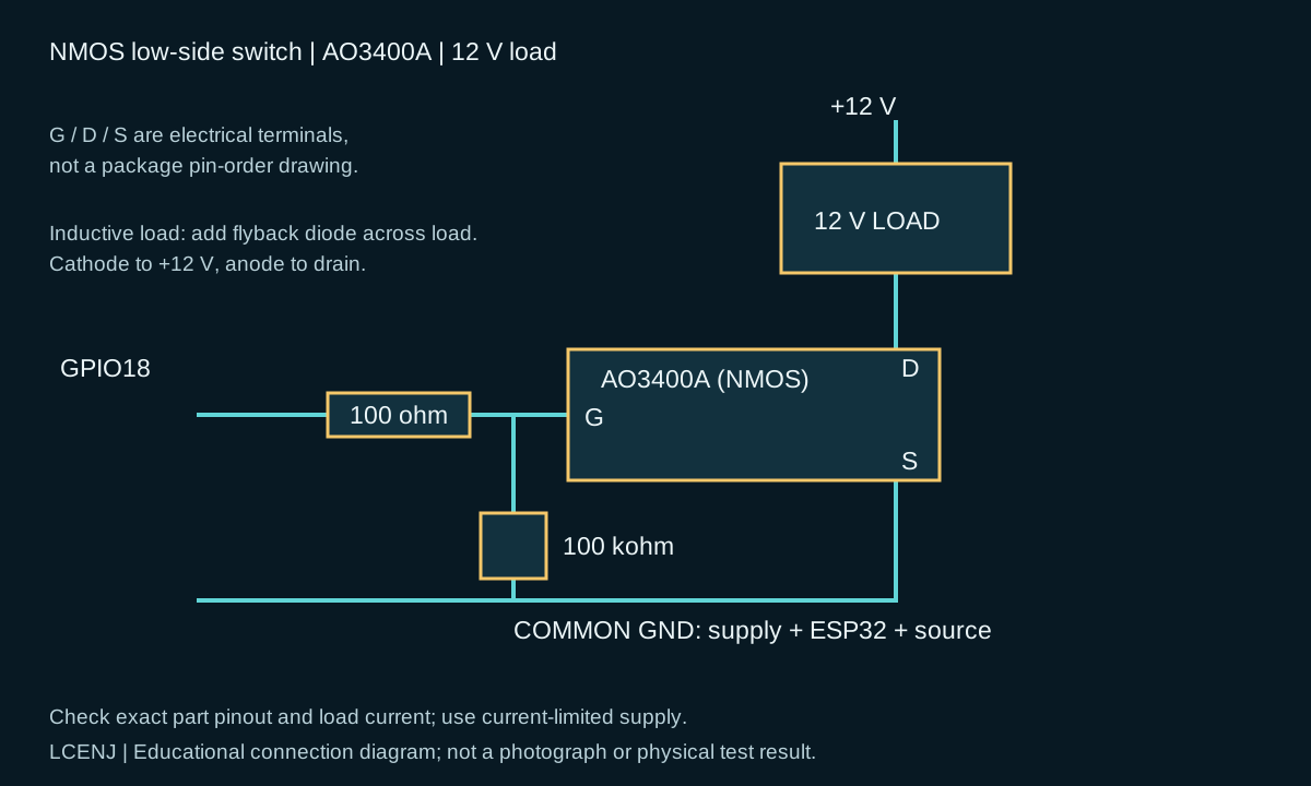
- Connect the positive of the 12V source to the positive of the load.
- Connect the negative charge to the Drain pin of the MOSFET.
- Connect the Source pin of the MOSFET to the ground of the 12V source.
- Connect the ESP32 ground to the same ground as the 12V source.
- Connect GPIO18 to Gate through 220 ohm resistor.
- Place a 100 kOhm resistor between Gate and Source.
- Set the source current limiter to a low value first and then connect the power supply.
Do not start the first test with the motor or pump
Use an LED strip or a resistive load to start. Inductive loads such as motors, pumps, relays and solenoid valves generate voltage when the pulse is interrupted and require a stray diode.
Simple command to test on and off
#include "driver/gpio.h"
#include "freertos/FreeRTOS.h"
#include "freertos/task.h"

#define MOSFET_GATE GPIO_NUM_18

void app_main(void)
{
    gpio_reset_pin(MOSFET_GATE);
    gpio_set_direction(MOSFET_GATE, GPIO_MODE_OUTPUT);
    gpio_set_level(MOSFET_GATE, 0);

    while (1) {
        gpio_set_level(MOSFET_GATE, 1);  // Load on
        vTaskDelay(pdMS_TO_TICKS(2000));

        gpio_set_level(MOSFET_GATE, 0);  // Load off
        vTaskDelay(pdMS_TO_TICKS(2000));
    }
}
What should we see?
| GPIO status | Approximate gate voltage compared to source | MOSFET behavior | load status |
|---|---|---|---|
| Zero | Approximately 0 volts | off | off |
| one | Approximately 3.3 volts | bright | bright |
Now let's extract the concept from the circuit
What exactly does Gate, Drain, Source and VGS mean in this circuit?
Gate
It is a command pin and receives signal from GPIO. It consumes almost no significant DC current in steady state, but must be charged and discharged when switching states.
Drain
In this circuit, it is connected to the negative charge. When the MOSFET turns on, the load current flows from Drain to Source.
Source
In the low-side circuit, it is connected to the ground and is considered the real reference of the gate voltage.
The most important point of the lesson
The MOSFET is controlled by the Gate to Source voltage. We call this voltage VGS. In our orbit the Source is on Earth; Therefore, Gate is equal to 3.3 volts, which means that VGS is approximately 3.3 volts.
Why did we put a resistance of 100 kilo ohms?
When the ESP32 is powered on or reset, the GPIO pin may be input for a few moments with no known status. Gate MOSFET can hold residual charge like a small capacitor. A 100 kOhm resistor pulls the Gate to the Source so that the MOSFET remains off by default.
Why did we put 220 Ohm resistance of Gate series?
When changing state, the GPIO must charge or discharge the gate capacitance. Series resistance limits the instantaneous current and helps reduce oscillation and noise. For this test, 220 ohms is a good value, but in fast PWM, the exact value should be checked with the gate load, frequency and required speed.
Read the datasheet only for real decisions
Why was the AO3400A chosen for this example?
We are not going to keep all the datasheets. We only ask questions that are necessary for the 12V circuit and the 3.3 V GPIO.
1. Does it withstand 12 volts?
In the data sheet, the value of VDS is equal to 30 volts. Therefore, in terms of nominal voltage, it is suitable for 12 V circuit; However, in inductive load, voltage pulses must be restrained.
2. Does it really turn on with a 3V gate?
The datasheet also specifies RDS(on) on resistance at VGS of 2.5V: about 48mOhms max. This is more important than VGS(th), because VGS(th) only indicates the onset of conduction with very low current.
3. Does the current of 1 amp cause heat?
Using the worst value of 48 milliohms, we calculate the conduction losses.
P = I² × R
P = 1² × 0.048
P = 0.048 W
About 48mW dissipation is low to begin with. But at 2 amps, the loss is quadrupled:
P = 2² × 0.048 = 0.192 W4. So what does the current number of 5.7 amps on the first page mean?
This number has been measured in specific thermal and range conditions. We should not conclude that every AO3400A on every PCB can pass 5.7 amps continuously without checking the temperature. Copper level, ambient temperature, assembly quality and current flow time are decisive.
5. What is the maximum gate voltage?
The absolute limit of VGS is ±12 volts. In the 3.3 V circuit, we are far from this limit.
| Datasheet parameter | Our practical question | The amount of AO3400A |
|---|---|---|
| VDS | Does it withstand 12 volts? | 30 volts |
| RDS(on) at VGS=2.5V | How much loss and heat do we have with three-volt GPIO? | Maximum 48 milliohm |
| RDS(on) at VGS=4.5V | What changes with a stronger drive? | Maximum 32 milliohm |
| VGS(max) | How much voltage does Gate not get damaged? | ±12 volts |
| Qg at 4.5V | How much is gate charge in PWM? | About 7 nanocoulombs |
| RθJA | How important are heat transfer and heat dissipation? | PCB dependent; About 125°/W in reference steady state |
Let's make the problem one step more difficult
Instead of just turning on and off, change the intensity of the light with PWM
Now we keep the same circuit and control the GPIO with PWM. The MOSFET turns the load on and off at a rate of several thousand times per second. The human eye sees the average light; So as the Duty Cycle changes, the brightness changes.
#define PWM_FREQUENCY_HZ 5000
#define PWM_MAX_DUTY     1023

static void pwm_set_percent(uint32_t percent)
{
    if (percent > 100) {
        percent = 100;
    }

    uint32_t duty = (PWM_MAX_DUTY * percent) / 100;
    ledc_set_duty(LEDC_LOW_SPEED_MODE, LEDC_CHANNEL_0, duty);
    ledc_update_duty(LEDC_LOW_SPEED_MODE, LEDC_CHANNEL_0);
}
Which new datasheet parameter becomes important here?
On slow on and off, gate capacitance wasn't nearly as big of an issue. In PWM, the Qg or Gate Charge parameter becomes important. The higher the Qg, the more charge the GPIO or driver has to move per cycle, and the longer the MOSFET transits through the half-on region.
Measurement test
Record the MOSFET input current and temperature at 25, 50, 75 and 100% duties. The measurement record file is inside the download package.
A real error in projects
What changes if our load is a pump, motor, relay or solenoid valve?
An inductive load stores energy when current flows. When the MOSFET suddenly turns off, this energy tries to keep the current flowing and can raise the drain voltage very high. For this reason, we put a diode parallel to the load.
The direction of the stray diode
In normal mode, the diode should be reversed; That is, the cathode should be connected to the positive side of the source and the anode should be connected to the drain or negative side of the load. The diode should be selected in terms of current, speed and energy with the load.
Here we realize that VDS equal to 30V alone is not enough guarantee. For 12 V inductive load, diode, TVS, short circuits and checking waveform with oscilloscope are important.
Problem number 2
Sometimes we don't want to disconnect the load; We have to stop feeding positively
Suppose a 5V sensor or module is connected to ESP32 and its data lines must have a common ground. If we cut power from the ground side with the NMOS, the signal paths may inadvertently feed the module through the data pins. A better way is to disconnect the positive 5V. This is where PMOS comes in.
Why didn't we connect the Gate directly to the ESP32?
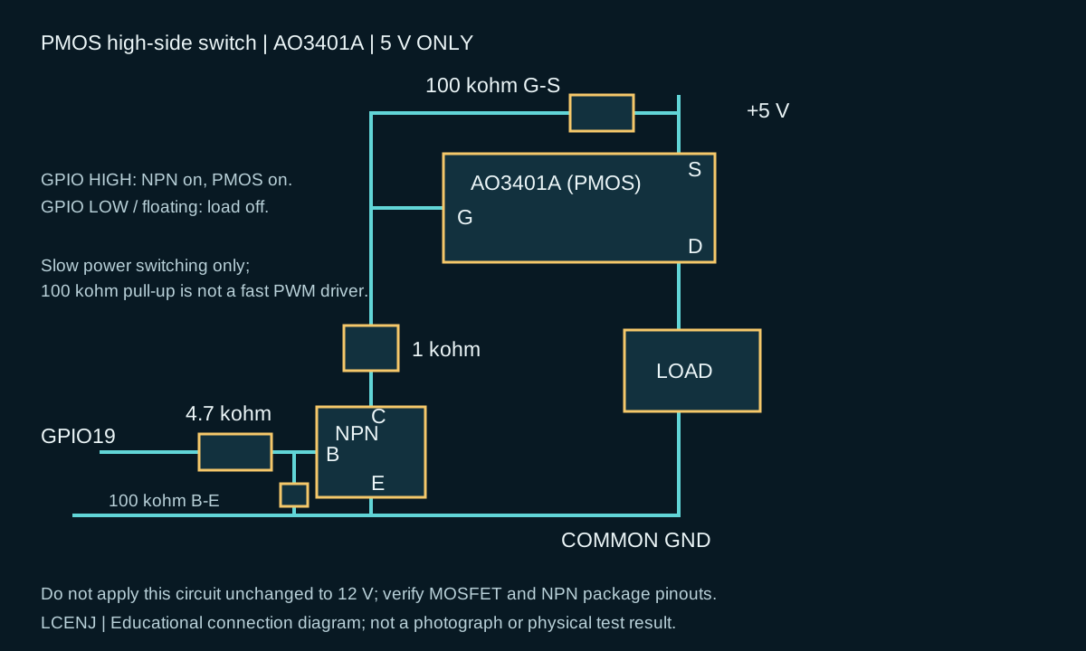
Source MOSFET is on 5V. For the PMOS to turn off, the Gate must reach approximately the same 5V; But the ESP32 GPIO outputs a maximum of 3.3V. If the Gate is directly connected to the GPIO, in the High state, VGS will be equal to 3.3 minus 5, that is, about negative 1.7 volts, and the MOSFET may not turn off completely. So a small NPN transistor pulls the gate down and the pull-up resistor pulls it back to the source when off.
Step by step connections
- Source Connect the AO3401A MOSFET to the positive 5V.
- Connect the drain to the positive of the load.
- Common the ESP32's negative load and ground.
- Place a 100 kOhm resistor between Gate and Source so that the default PMOS is off.
- Connect the Gate to the NPN collector through a 1 kOhm resistor.
- Connect the NPN emitter to ground.
- Connect GPIO19 to the NPN base through a 4.7 kOhm resistor.
- Place a 100 kOhm resistor between the base and emitter of the NPN so that the path remains off by default when the GPIO is floating.
The 100 kohm Gate-Source resistance is for slow connection and disconnection of the power supply; This is not a fast PWM driver circuit. Test behavior during reset, load inrush current and feed back from data lines separately. No physical test of this circuit is claimed in this article.
static void load_power_set(bool enabled)
{
    // In this circuit, GPIO=1 turns on the NPN, which then turns on the PMOS.
    gpio_set_level(GPIO_NUM_19, enabled ? 1 : 0);
}
Second datasheet, just for this circuit
Let's review AO3401A with practice questions
| question | parameter | AO3401A datasheet answer |
|---|---|---|
| Does the rail withstand 5 volts? | VDS | minus 30 volts |
| How much resistance is there in VGS of about minus 5 volts? | RDS(on) at −4.5V | Maximum about 60 milliohms |
| Can it be used in low voltage rail? | RDS(on) at −2.5V | Maximum about 85 milliohms |
| What is Gate's damage limit? | VGS(max) | ±12 volts |
| How much load does it have for gate switching? | Qg at 4.5V | About 7 nanocoulombs |
Loss calculation for 800 mA load
P = I² × R
P = 0.8² × 0.060
P ≈ 0.038 W
Do not repeat the same circuit without changing to 12 volts
If the Source is at 12V and pulls the NPN Gate down to zero, VGS will be approximately negative 12V; That is, exactly on the absolute limit of the data sheet. In the actual product, a zener clamp, limiting grid or high-side driver should be considered.
Summary based on application
When to choose NMOS and when to choose PMOS?
| circuit needs | The usual choice | the reason |
|---|---|---|
| Motor, LED, relay or pump control from the ground side | NMOS Low-side | Simple drive with GPIO and usually less on resistance |
| Fast PWM and low loss | NMOS | Usually has better selections and lower RDS(on). |
| Positive interruption of the power supply of a module | PMOS High-side | The land remains a shared burden |
| High-side with high voltage or current and fast PWM | NMOS with High-side driver | Better efficiency than PMOS, but more complex circuit |
practical exercise
This lesson is over when you measure the numbers
- In NMOS circuit, measure VGS in off and on state.
- In the ON state, measure VDS and calculate the approximate resistance of the path with the relation R≈VDS/I.
- Record the load current at 25, 50, 75 and 100% duties.
- After five minutes of operation, check the temperature of the MOSFET and the temperature of the copper around it.
- Turn off the source, deliberately match the Drain and Source to the pinout map, and check the direction of the body diode in the Diode Test mode.
- Run the PMOS circuit and measure VGS in two GPIO modes zero and one.
- Disconnect and reconnect the positive load wire and check that the load ground remains common.
The main purpose of the exercise
The student should be able to explain from measured voltages why an NMOS or PMOS turns on and off without memorizing definitions.
troubleshooting
If the circuit does not work, proceed with this procedure
- Check common ground. In NMOS circuit, ESP32 ground and load source must be common.
- Match the actual pinout of the part with the datasheet. Do not guess the SOT-23 pin order from the appearance.
- Measure VGS, not just gate voltage to ground.
- Gate should not float. Check Pull-down for NMOS and Pull-up to Source for PMOS.
- The source has not entered the flow limiter.
- Measure the on state VDS. A high value means that the MOSFET is not completely turned on, the part is bad, or the connection is wrong.
- For inductive load, check the stray diode and its direction.
- In PMOS, don't get the logic circuit wrong. Gate going low relative to Source causes it to turn on.
MOSFET selection formula for next project
Before choosing a piece, just answer these seven questions:
- What is the actual drain-source voltage and possible pulses?
- What is the continuous current and the current at the start of the load?
- How many volts will the actual VGS be in the circuit?
- What is the RDS(on) at the same VGS?
- What is the I²R loss and temperature rise?
- What is the switching frequency and Qg?
- Is the load resistive or inductive and what protections does it need?
Download ESP-IDF codes, AO3400A and AO3401A datasheet, BOM and measurement record sheet
What we learned practically in this lesson
We started with a small problem, connected the AO3400A as a low-side NMOS, extracted VGS and RDS(on) from the datasheet when needed, added PWM, recognized the risk of inductive load, and then built a high-side PMOS circuit with the AO3401A for switching the positive supply rail. Now datasheet parameters are no longer a set of numbers separate from the circuit; Each parameter is the answer to a real design question.
Question and answer article
Ask your technical question
Questions and answers are published after moderation. Authors can see their own pending drafts.
No confirmed questions have been registered for this article yet.